Supercharge Your Innovation With Domain-Expert AI Agents!

Photomask and pattern formation method using the same

Inactive Publication Date: 2009-03-05
PANNOVA SEMIC
View PDF17 Cites 14 Cited by
  • Summary
  • Abstract
  • Description
  • Claims
  • Application Information

AI Technical Summary

Benefits of technology

"The present invention provides a photomask that can prevent the occurrence of a side lobe and a resist defect when using an enhancer mask to form isolated contact patterns and densely arranged contact patterns. The photomask includes a semi-light-shielding portion, a first opening, a second opening, and a phase-shifting portion. The first and second openings have different dimensions, and the phase-shifting portion is designed to transmit the exposing light in an opposite phase to the first opening. The use of this photomask can prevent the formation of an insoluble layer that causes a resist defect and improve the resolution capability and prevent degradation of the depth of focus."

Problems solved by technology

In the case where the method disclosed in Patent Document 1 is used in combination with the enhancer mask, however, there arises a problem that a resist defect is caused around a portion on a wafer corresponding to the large opening such as the accessory pattern.
This problem is serious in employing ArF exposure process and particularly ArF immersion exposure process.

Method used


Image

  • Photomask and pattern formation method using the same
  • Photomask and pattern formation method using the same
  • Photomask and pattern formation method using the same

Examples


embodiment

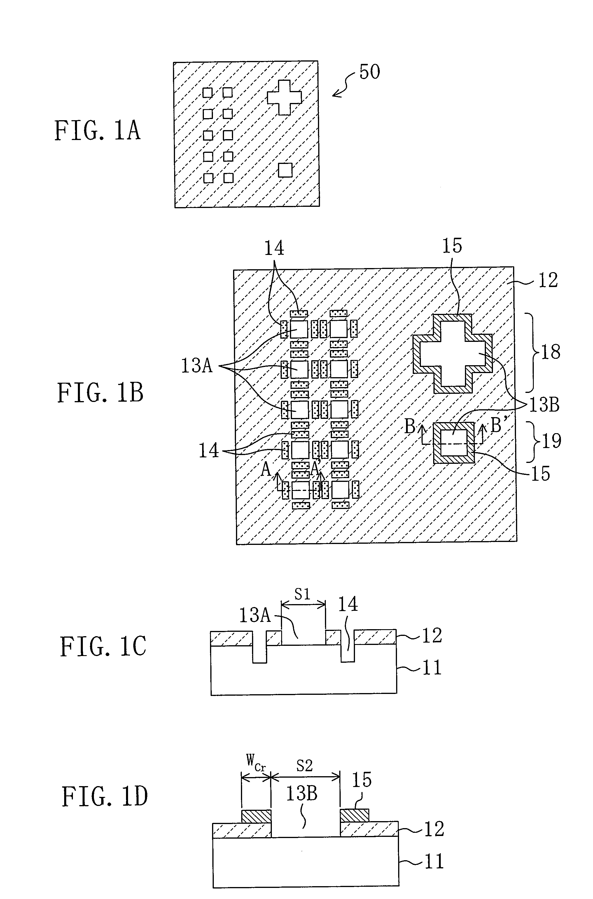
[0056]A photomask according to an embodiment of the invention will now be described with reference to the accompanying drawings.

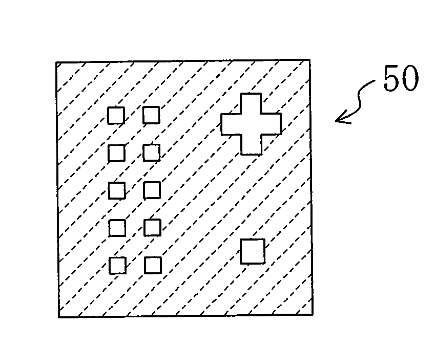
[0057]FIG. 1A shows an example of a pattern to be formed by using the photomask according to the embodiment of the invention. Also, FIG. 1B is a plan view of an example of the photomask of this embodiment, and more specifically, an example of an enhancer mask used for forming a desired pattern 50 shown in FIG. 1A, FIG. 1C is a cross-sectional view taken on line A-A′ of FIG. 1B and FIG. 1D is a cross-sectional view taken on line B-B′ of FIG. 1B.

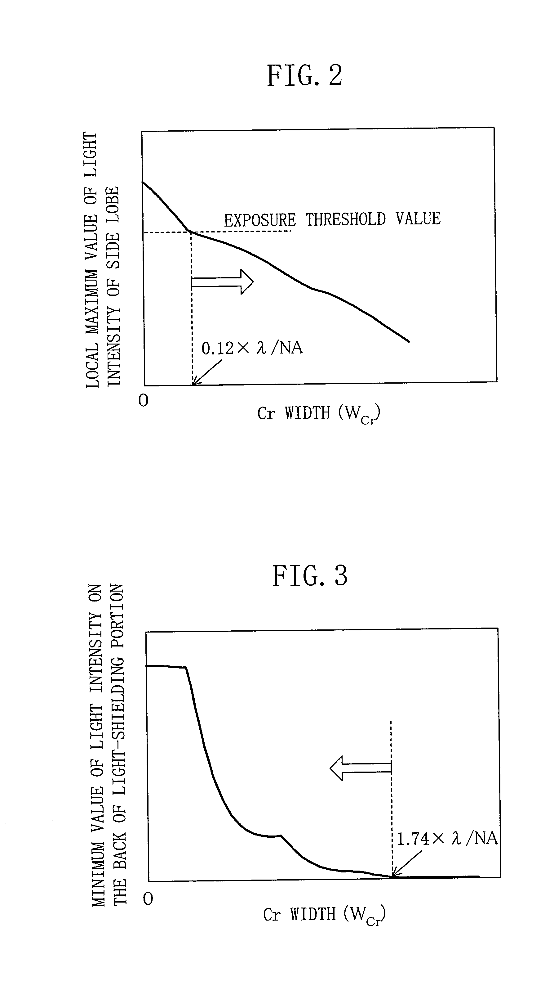
[0058]As shown in FIGS. 1B through 1D, in a semi-light-shielding portion 12 formed on the transparent substrates and partially transmits exposing light, first openings 13A each having a first dimension S1 not more than, for example, (0.5×λ / NA)×M and second openings 13B each having a second dimension S2 larger than, for example, (0.5×λ / NA)×M are formed. A phase-shifting portion 14 is formed on the transparent substrate...


PUM

PropertyMeasurementUnit
widthaaaaaaaaaa
hole sizeaaaaaaaaaa
hole sizeaaaaaaaaaa

Abstract

A photomask includes a transparent substrate having a transparent property against exposing light, a semi-light-shielding portion formed on the transparent substrate, a first opening formed in the semi-light-shielding portion and having a first dimension and a second opening formed in the semi-light-shielding portion and having a second dimension lager than the first dimension. A phase-shifting portion which transmits the exposing light in an opposite phase with respect to the first opening is formed on the transparent substrate around the first opening. A light-shielding portion is formed on the transparent substrate around the second opening.

Description

BACKGROUND OF THE INVENTION[0001]1. Field of the Invention[0002]The present invention relates to a photomask used for forming a fine pattern in fabrication of a semiconductor integrated circuit device and a pattern formation method using the photomask.[0003]2. Description of Related Art[0004]Recently, there are increasing demands for refinement of a circuit pattern due to a high degree of integration of a large scale integrated circuit device (hereinafter referred to as an LSI) realized by using a semiconductor. As a result, great importance is placed on refinement of a wiring pattern forming the circuit or a contact hole pattern for connecting multiple wiring layers with insulating layers interposed therebetween (hereinafter referred to as a contact pattern). For the formation of the contact pattern, a technique of simultaneously forming isolated patterns and densely arranged patterns has been required. For achieving large depth of focus in the formation of the densely arranged con...

Claims


Application Information

Patent Timeline
Patent Type & Authority Applications(United States)
IPC IPC(8): G03F1/00G03F7/22G03F1/29G03F1/32G03F1/68H01L21/027
CPCG03F1/144G03F1/36G03F1/26G03F1/29G03F1/32
Inventor IRIE, SHIGEOMISAKA, AKIONONAMI, YUJINAKAMURA, TETSUYAHARADA, CHIKA
Owner PANNOVA SEMIC
Features
  • R&D
  • Intellectual Property
  • Life Sciences
  • Materials
  • Tech Scout
  • Unparalleled Data Quality
  • Higher Quality Content
  • 60% Fewer Hallucinations
Learn More