Printed circuit board

Inactive Publication Date: 2009-03-12
HON HAI PRECISION IND CO LTD
View PDF8 Cites 3 Cited by
  • Summary
  • Abstract
  • Description
  • Claims
  • Application Information

AI Technical Summary

Problems solved by technology

However, in this broadside-coupling mode of the conventional PCB 1, the single-ended impedance of either of the positive

Method used


Image

  • Printed circuit board
  • Printed circuit board
  • Printed circuit board

Examples


Embodiment Construction

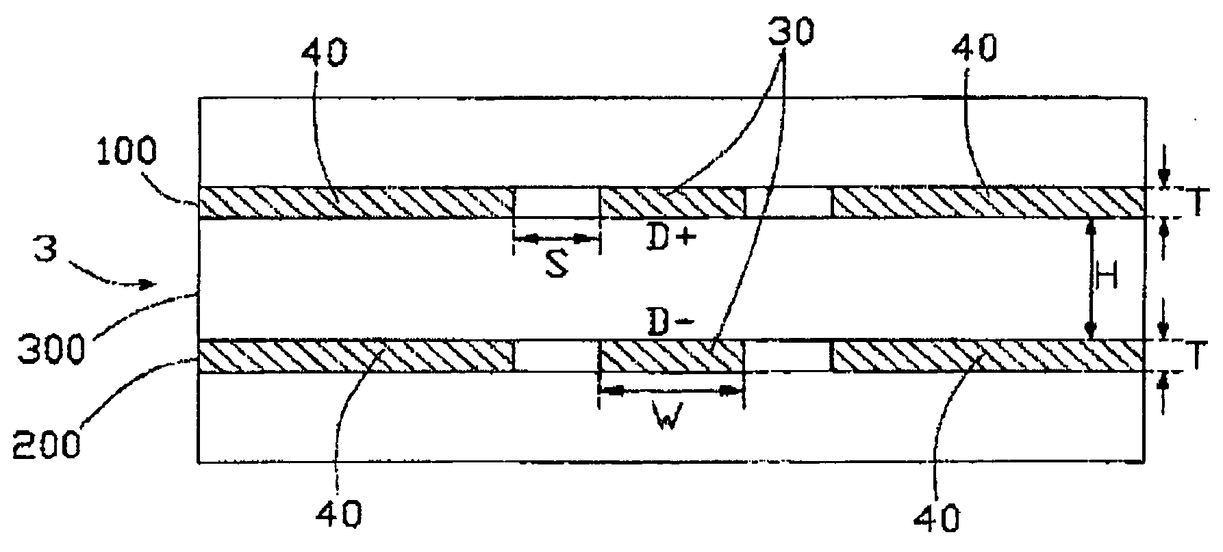
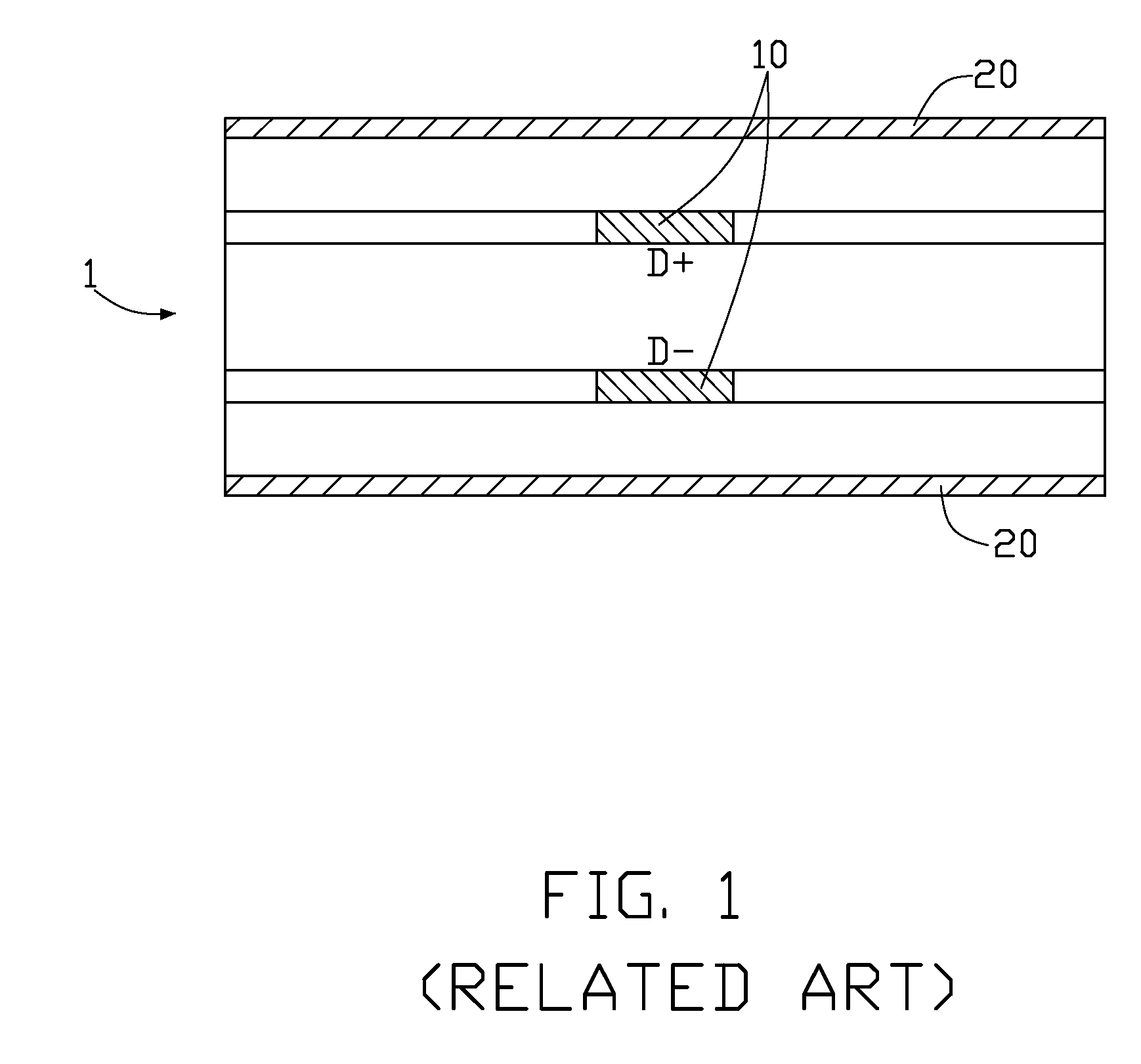
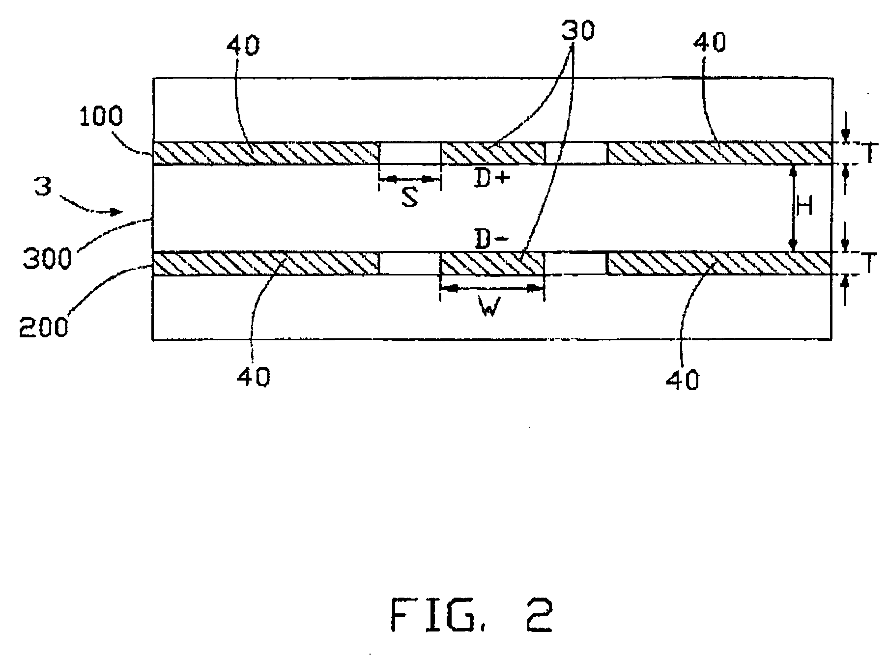
[0011]Referring to FIG. 2, a printed circuit board (PCB) 3 in accordance with an embodiment of the present invention includes a differential pair 30 having a positive differential trace D+ and a negative differential trace D− respectively disposed within two signal layers sandwiching a dielectric layer therebetween, two ground parts 40 respectively arranged at opposite sides of the positive differential trace D+, and two ground parts 40 respectively arranged at opposite sides of the negative differential trace D−.

[0012]A single-ended impedance of a signal trace of the differential pair 30 can be calculated with this formula:

Z0≈87ɛr+1.41ln5.98S0.8W+T

Wherein, Z0 is the single-ended impedance of the signal trace, ∈r is the dielectric constant, W is the width of the signal trace, T is the thickness of the signal trace, S is the distance between the signal trace and the adjacent ground part 40. The single-ended impedance of the signal trace can be adjusted by changing the width W, the th...


PUM


Abstract

A printed circuit board (PCB) includes first and second signal layers sandwiching a dielectric layer therebetween, and a differential pair having two differential traces respectively disposed within the first and second signal layers. Two ground parts are respectively arranged at opposite sides of each of the two differential traces.

Description

BACKGROUND[0001]1. Field of the Invention[0002]The present invention relates to printed circuit boards (PCBs), and particularly to a PCB with reduced single-ended impedances of signal traces thereof.[0003]2. Description of Related Art[0004]Referring to FIG. 1, a partial cross-sectional view of a conventional PCB 1 is illustrated. As shown, the PCB 1 includes a differential pair 10 having a positive differential trace D+ and a negative differential trace D− respectively disposed within two signal layers in a broadside-coupling mode, and two ground layers 20 arranged above and below the differential pair 10 respectively. A preferred value of the differential impedance between the positive differential trace D+ and negative differential trace D− is approximately 100 ohms, and a preferred value of the single-ended impedance of either of the positive differential trace D+ and negative differential trace D− is approximately 50˜60 ohms.[0005]However, in this broadside-coupling mode of the ...

Claims


Application Information

Patent Timeline
IPC IPC(8): H05K1/02
CPCH05K1/0219H05K2201/09672H05K2201/09336H05K1/0245
Inventor LIU, CHIEN-HUNGHSU, SHOU-KUOPAI, YU-CHANG
Owner HON HAI PRECISION IND CO LTD
Why Eureka
Try Eureka