Impedance adjusting circuit and impedance adjusting method

a technology of impedance adjustment and impedance adjustment, which is applied in the direction of logic circuit coupling/interface arrangement, pulse technique, instruments, etc., can solve the problems of adversely affecting the characteristics of ddr2 memory, difficult to make the impedance adjustment based on an absolute value, and ineffective means for making the impedance adjustment of the output buffer in the ddr2 memory. , to achieve the effect of facilitating the impedance adjustment of the output buffer

Inactive Publication Date: 2009-06-16
RENESAS ELECTRONICS CORP
View PDF2 Cites 3 Cited by
  • Summary
  • Abstract
  • Description
  • Claims
  • Application Information

AI Technical Summary

Benefits of technology

[0045]According to the present invention, impedance adjustment of the output buffer in the DDR2 memory or the like from a side of the memory controller is facilitated.

Problems solved by technology

As described above, there is no effective means for making the impedance adjustment of the output buffer in the DDR2 memory, using the OCD impedance adjusting function, from the memory controller side.
Thus, the impedance adjustment based on an absolute value has been made extremely difficult.
When the impedance adjustment of the output buffer in the DDR2 memory cannot be made, an unbalance between the impedances of the pull-up buffer and the pull-down buffer that output the differential strobe signals (DQS, DQSB) for data control, respectively, which are output from the DDR2 memory to the memory controller, is seen as the jitter in the memory controller, thereby adversely affecting the characteristics of the DDR2 memory.

Method used


Image

  • Impedance adjusting circuit and impedance adjusting method
  • Impedance adjusting circuit and impedance adjusting method
  • Impedance adjusting circuit and impedance adjusting method

Examples


Embodiment Construction

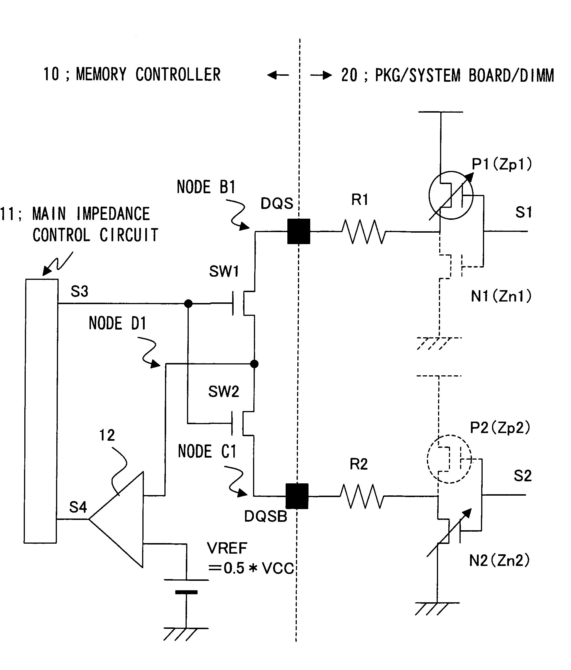
[0059]The preferred embodiments of the present invention with be described with reference to appended drawings. In the present invention, by comparing impedances of a pull-up output buffer and a pull-down output buffer using complementary output signals such as differential strobe signals (DQS, DQSB) for data control from a DDR2 memory side, using an OD impedance adjusting function of a DDR2 memory, relative impedance adjustment is made. Since the relative impedance adjustment is made, series resistance components on the package / system board / DIMM are compensated and prohibited from influencing the impedance adjustment.

[0060]Generally, lengths of wiring for important signals that determine an operating speed of a system, such as a data signal (DQ) and the differential strobe signals (DQS, DQSB) for data control, are made equal on the package / system board / DIMM so that delays thereof are equal.

[0061]FIG. 1 is a diagram showing a configuration of an embodiment of the present invention. ...


PUM


Abstract

An impedance adjusting circuit for adjusting an impedance of an output buffer of a DDR2 memory, using an OCD impedance adjusting function, from a side of a memory controller, includes first and second terminals, first and second switches, a comparator, and a control circuit. The DDR2 memory has an OCD impedance adjusting function and includes a first output buffer and a second buffer each having a pull-up buffer and a pull-down buffer that receive an input signal in common and with impedances thereof capable of being variably set. The first and second terminals receive first and second signals output from the first buffer and the second buffers, respectively. The first and second switches are connected between the first terminal and the second terminal in series. The comparator compares a reference voltage VREF with a voltage at a connection node between the first and second switches. The control circuit receives a comparison result from the comparator to perform control for adjustably setting the impedance of the first buffer and / or the impedance of the second buffer, and also performs on / off control of the first and second switches.

Description

FIELD OF THE INVENTION[0001]The present invention relates to an impedance adjusting circuit and an impedance adjusting method.BACKGROUND OF THE INVENTION[0002]The present invention is suitably applied to impedance adjustment of an output buffer of a DDR (Double Data Rate) 2 memory having an OCD (Off-Chip Driver) impedance adjusting function in a memory interface. A background art of the present invention will be described below.[0003]As a conventional approach to OCD impedance adjustment, the impedance adjustment of an output buffer of a memory controller connected to the DDR2 memory will be described below. In the case of the output buffer of the memory controller, there is no influence of a series resistance on a package (PKG) / system board / DIMM (Dual Inline Memory Module) and hence the impedance adjustment can be performed with relative ease. A method of adjusting an impedance of an output buffer in a memory controller 10 shown in FIG. 11 will be described. FIG. 12A through FIG. 1...

Claims


Application Information

Patent Timeline
Patent Type & Authority Patents(United States)
IPC IPC(8): H03K19/013H03K19/003
CPCG11C7/1048G11C7/1051G11C7/1057G11C7/1066G11C11/4093G11C29/02G11C29/022G11C29/028G11C29/50008H03K19/0005G11C11/401G11C2207/2254H03K19/017545
Inventor KUROKI, KOUICHI
Owner RENESAS ELECTRONICS CORP
Why Eureka
Try Eureka