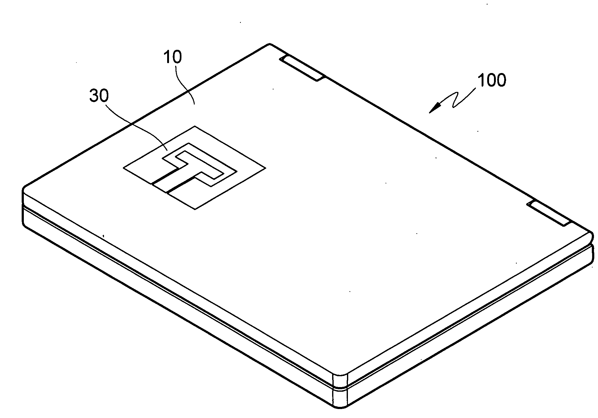
Case structure of electronic device
a technology of electronic devices and cases, applied in the direction of protective materials, antenna details, protective materials radiating elements, etc., can solve the problem of original whole volume of electronic devices, and achieve the effect of improving the space utilization rate of electronic devices
- Summary
- Abstract
- Description
- Claims
- Application Information
AI Technical Summary
Benefits of technology
Problems solved by technology
Method used
Image

Examples
Embodiment Construction
[0045]A case structure of an electronic device according to the present invention is used for accommodating an internal circuit of the electronic device. Herein, the electronic device can be, but not limited to, personal digital assistant (PDA), mobile phone, smart phone, PDA phone, notebook computer or the like. The accompanying drawings are used for providing reference and illustration, but not for limiting the present invention.
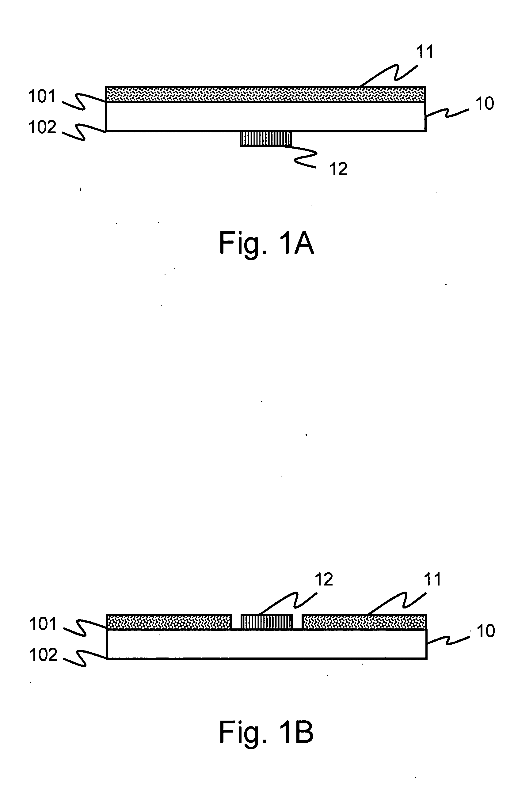
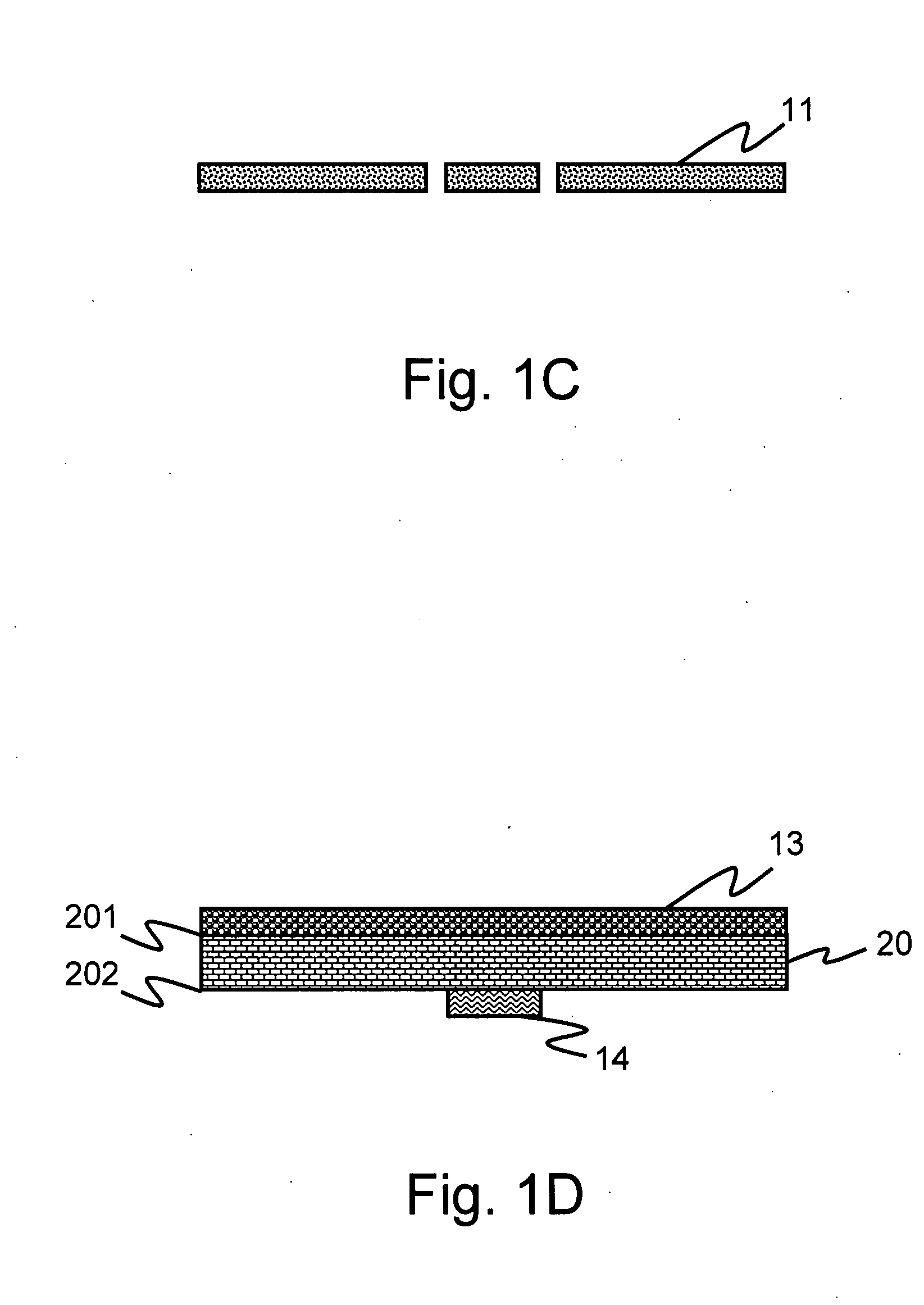
[0046]Referring to FIG. 1A, a schematic sectional structural view of a first embodiment according to the present invention is shown. As shown in FIG. 1A, the case structure of the present invention includes a dielectric layer 10, a metal case 11, and a metal layer 12.
[0047]The dielectric layer 10 has a first surface 101 and a second surface 102, and the dielectric layer 10 can be, for example, ceramic material.
[0048]The metal case 11 is used for holding the internal circuit (not shown) and is disposed on the first surface 101 of the dielectric layer 10 to ...
PUM
 Abstract
Description
Claims
Application Information
 - R&D
- Intellectual Property
- Life Sciences
- Materials
- Tech Scout
- Unparalleled Data Quality
- Higher Quality Content
- 60% Fewer Hallucinations
Browse by: Latest US Patents, China's latest patents, Technical Efficacy Thesaurus, Application Domain, Technology Topic, Popular Technical Reports.
© 2025 PatSnap. All rights reserved.Legal|Privacy policy|Modern Slavery Act Transparency Statement|Sitemap|About US| Contact US: help@patsnap.com