Substrate processing apparatus, substrate transfer apparatus, substrate clamp apparatus, and chemical liquid treatment apparatus

a technology for clamping apparatus and substrates, which is applied in the direction of lapping machines, manufacturing tools, transportation and packaging, etc., can solve the problems of conventional substrate clamping apparatuses that cannot securely hold substrates of different sizes, and achieve the effects of small number of components, easy maintenance operations, and short tact time of substrate processing

Inactive Publication Date: 2009-03-12
EBARA CORP
View PDF14 Cites 64 Cited by
  • Summary
  • Abstract
  • Description
  • Claims
  • Application Information

AI Technical Summary

Benefits of technology

[0008]The present invention has been made in view of the above drawbacks. It is therefore a first object of the present invention to provide a substrate processing apparatus which can improve a tact time of processing a substrate.
[0009]It is a second object of the present invention to provide a substrate processing apparatus which can facilitate maintenance operations.
[0010]It is a third object of the present invention to provide a substrate transfer apparatus which has a small number of components and a simple structure and can achieve a low cost.

Problems solved by technology

However, a conventional substrate clamp apparatus has a problem in securely holding substrates of different sizes.

Method used


Image

  • Substrate processing apparatus, substrate transfer apparatus, substrate clamp apparatus, and chemical liquid treatment apparatus
  • Substrate processing apparatus, substrate transfer apparatus, substrate clamp apparatus, and chemical liquid treatment apparatus
  • Substrate processing apparatus, substrate transfer apparatus, substrate clamp apparatus, and chemical liquid treatment apparatus

Examples


Embodiment Construction

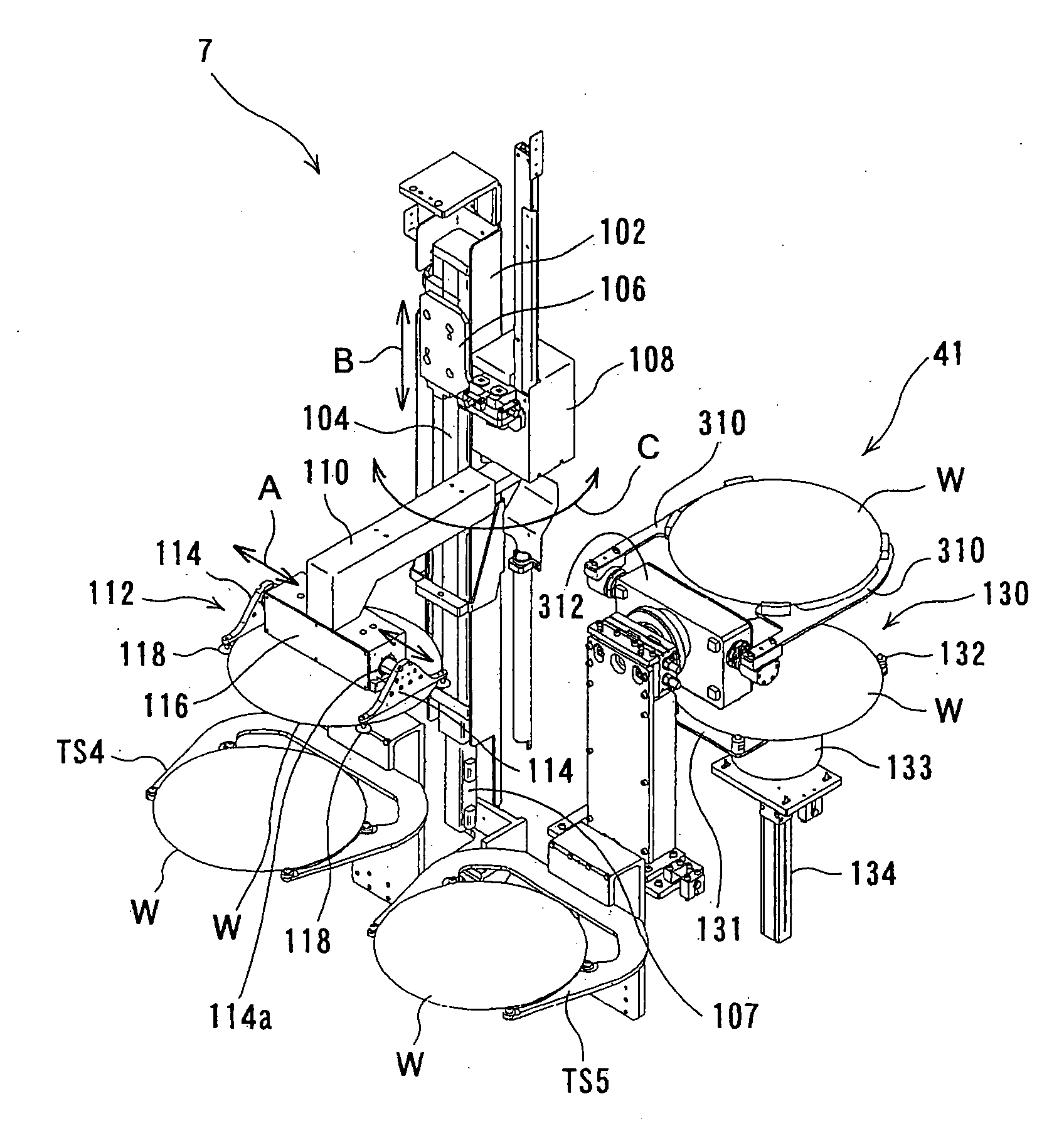
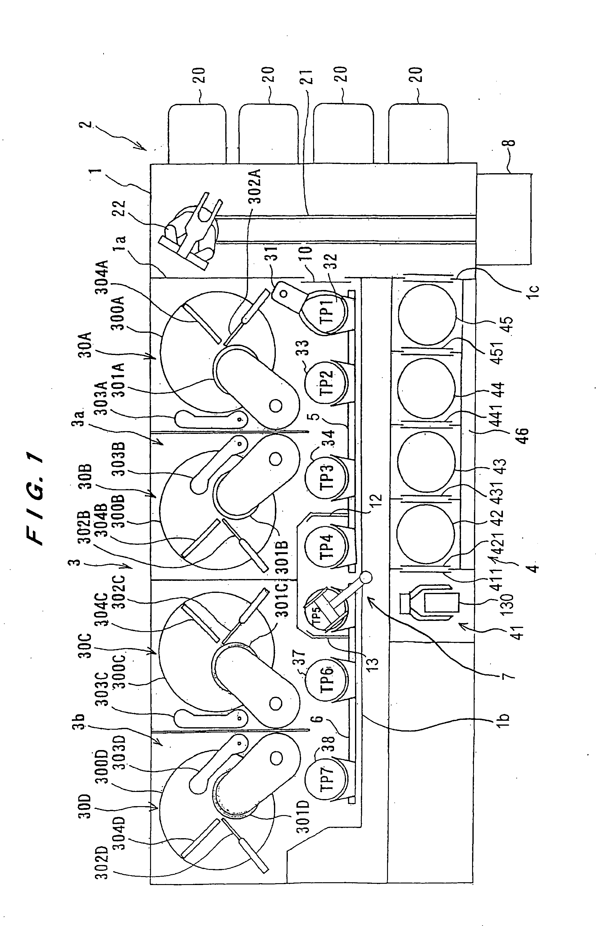
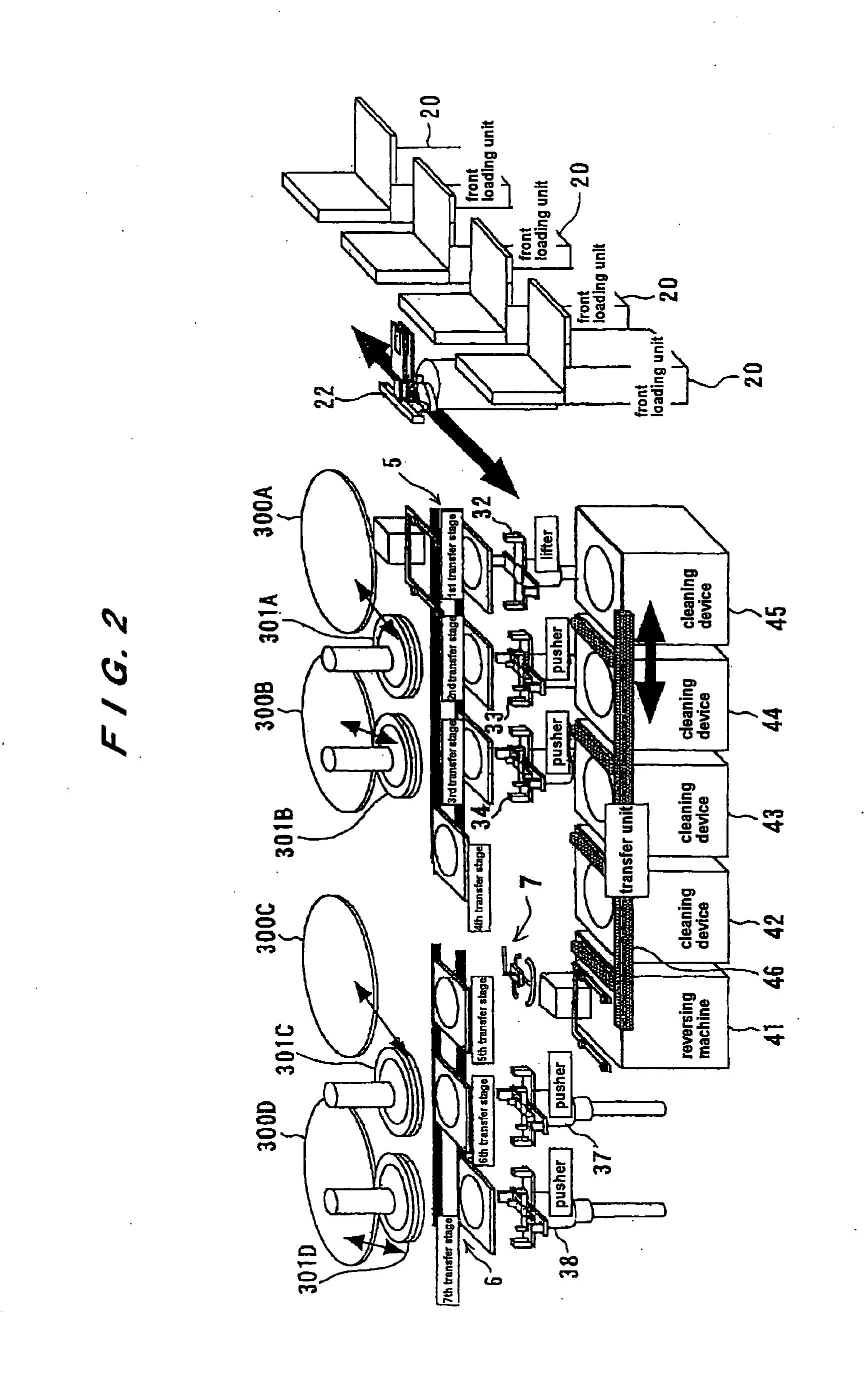
[0105]A polishing apparatus according to embodiments of the present invention will be described below in detail with reference to FIGS. 1 through 63. Identical or corresponding elements are denoted by the same reference numerals, and will not be described repetitively.

[0106]FIG. 1 is a plan view showing an entire arrangement of a polishing apparatus according to an embodiment of the present invention, and FIG. 2 is a perspective view showing an outline of the polishing apparatus shown in FIG. 1. As shown in FIG. 1, the polishing apparatus of the present embodiment has a housing 1 in a rectangular form. An interior space of the housing 1 is divided into a loading / unloading section 2, a polishing section 3 (3a, 3b), and a cleaning section 4 by partition walls 1a, 1b, and 1c. The loading / unloading section 2, the polishing sections 3a and 3b, and the cleaning section 4 are assembled independently of each other, and evacuation of gas from these sections is performed independently of each...


PUM


Abstract

The present invention relates to a substrate processing apparatus which can improve a tact time of substrate processing. A polishing apparatus as the substrate processing apparatus includes plural polishing sections (3a, 3b) each for polishing a semiconductor wafer (W), and a swing transporter (7) for transferring the wafer (W). The swing transporter (7) includes a wafer clamp mechanism (112) adapted to clamp the wafer (W), a vertically moving mechanism (104, 106) for vertically moving the wafer clamp mechanism (112) along a frame (102) of a casing of the polishing section (3a), and a swing mechanism (108, 110) for swinging the wafer clamp mechanism (112) about a shaft adjacent to the frame (102).

Description

TECHNICAL FIELD[0001]The present invention relates to a substrate processing apparatus, and more particularly to a substrate processing apparatus for polishing a substrate, such as a semiconductor wafer, to a flat mirror finish. The present invention also relates to a substrate transfer apparatus for use in such a substrate processing apparatus. Further, the present invention relates to a substrate clamp apparatus for use in such a substrate transfer apparatus and a reversing machine. Furthermore, the present invention relates to a chemical-liquid treatment apparatus for use in the above-mentioned substrate processing apparatus.BACKGROUND ART[0002]As semiconductor devices have become more highly integrated in recent years, circuit interconnects have become finer and distances between those interconnects have become smaller. In photolithography capable of forming interconnects with not more than 0.5 μm in wide, surfaces, on which pattern images are to be focused by a stepper, are req...

Claims


Application Information

Patent Timeline
Patent Type & Authority Applications(United States)
IPC IPC(8): H01L21/67B24B37/34
CPCB24B37/345H01L21/6719H01L21/67219H01L21/67742H01L21/68707H01L21/67748H01L21/67751H01L21/67766H01L21/67745H01L21/67196H01L21/6835H01L21/68721
Inventor TAKAHASHI, NOBUYUKINISHIDA, HIROAKITORII, HIROOMIISOBE, SOICHISONE, TADAKAZUKOSUGE, RYUICHIKANEKO, HIROYUKISOTOZAKI, HIROSHIMITSUKURA, TAKAOOGAWA, TAKAHIROSUGITA, KENICHI
Owner EBARA CORP
Why Eureka
Try Eureka