

Method of reducing wire bond profile height in integrated circuits mounted to circuit boards
a technology of integrated circuits and profile heights, which is applied in the direction of basic electric elements, solid-state devices, manufacturing tools, etc., can solve the problems of encapsulant bead hiccup, encapsulant volume and placement on the die is not very accurate, and the bead of encapsulant is not straigh
- Summary
- Abstract
- Description
- Claims
- Application Information
AI Technical Summary
Benefits of technology
Problems solved by technology
Method used
Image

Examples
Embodiment Construction
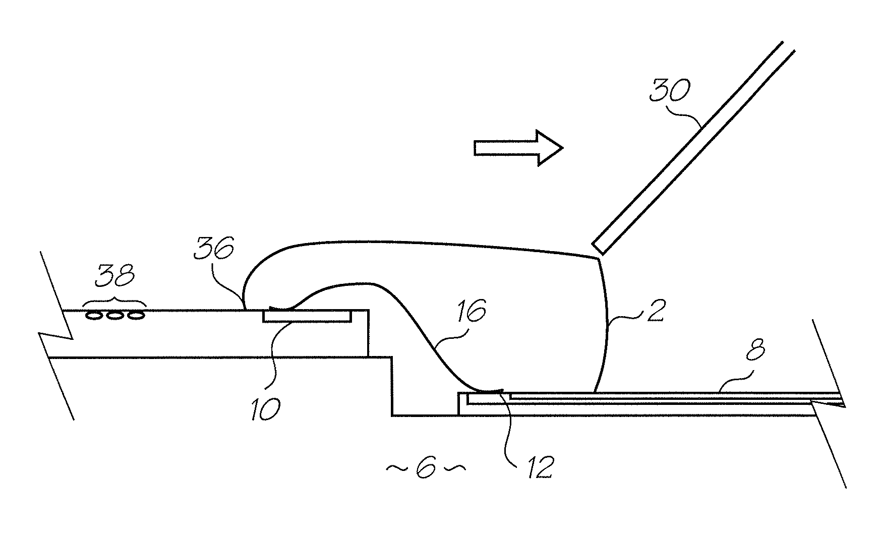
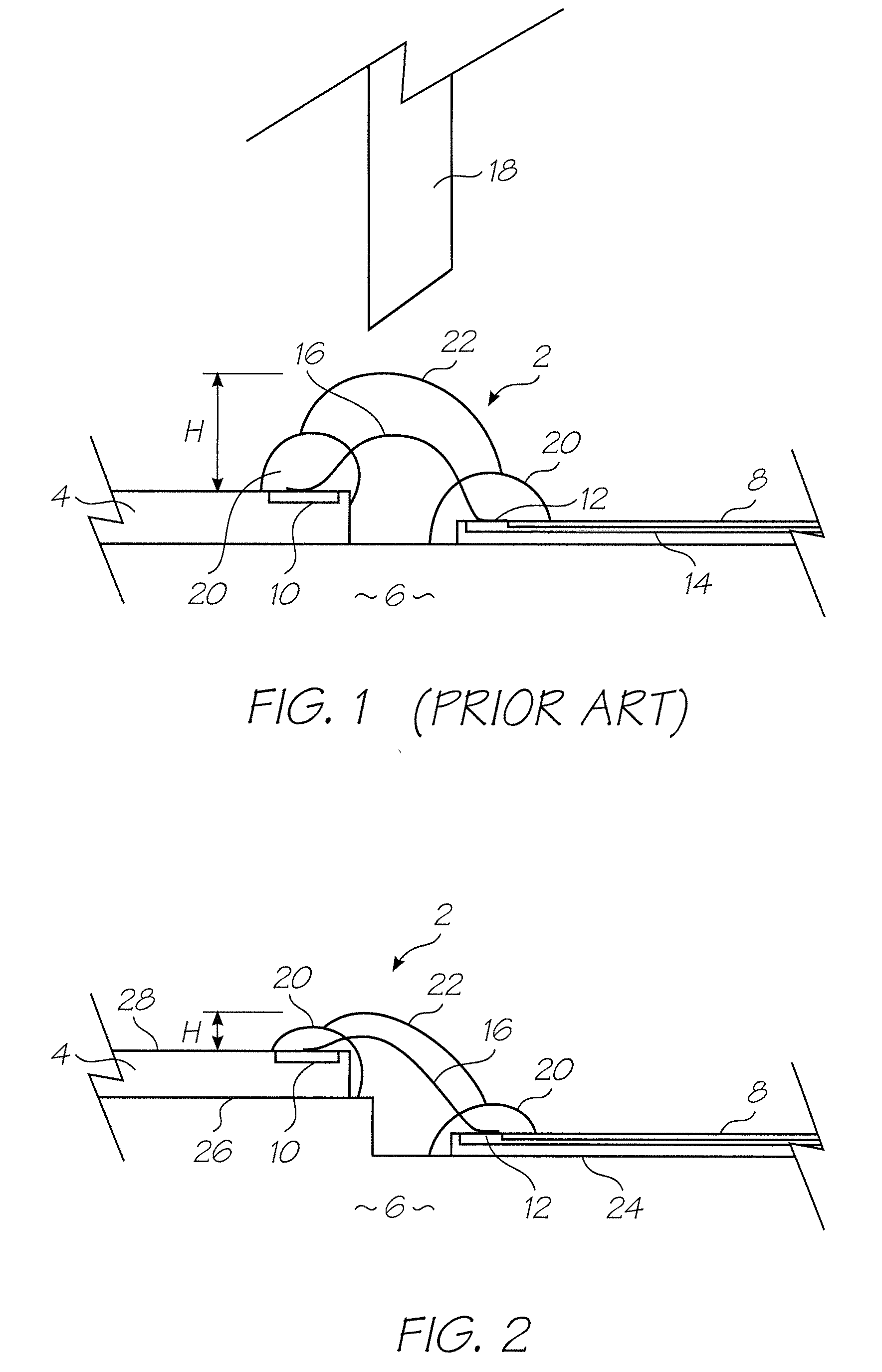
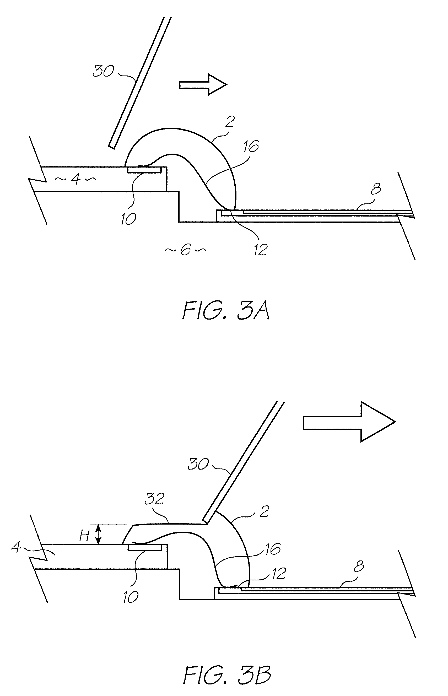
[0119]FIG. 1 shows a common technique used for applying a bead encapsulant to wire bonds. A die 4 is mounted to a supporting structure 6 adjacent the edge of a flex PCB 8 (flexible printed circuit board). The die 4 has a line of contact pads 10 along one edge and the flex PCB 8 has corresponding bond pads 12. Wire bonds 16 extend from the bond pads 10 to the bonds pads 12. Power and data is transmitted to the die 4 via conductive traces 14 in the flex PCB 8. This is a simplified representation of the dies mounted within many electronic devices. The printhead IC dies mounted to the LCP (liquid crystal polymer) molding to receive print data from an adjacent flex PCB, as described in U.S. Ser. No. ______ (Our Docket RRC001US) incorporated herein by cross reference, is one example of this type of die mounting arrangement. The ordinary worker will appreciate that the die may also be mounted directly to a hard PCB with traces formed thereon.
[0120]The wire bonds 16 are covered in a bead on...
PUM
| Property | Measurement | Unit |
|---|---|---|
| Length | aaaaa | aaaaa |
| Length | aaaaa | aaaaa |
| Length | aaaaa | aaaaa |
Abstract
Description
Claims
Application Information