

Semiconductor device having vertical surrounding gate transistor structure, method for manufacturing the same, and data processing system
a semiconductor device and surrounding gate technology, applied in the field of semiconductor devices having a vertical surrounding gate transistor (sgt) structure, semiconductor device manufacturing methods, data processing systems, etc., can solve the problems of difficult to realize highly integrated and high-performance semiconductor devices, difficult to control the threshold voltage of transistors, and become difficult to simply refine transistors. , to achieve the effect of quick responsiveness, low power consumption semiconductor devices, and quick responsiveness
- Summary
- Abstract
- Description
- Claims
- Application Information
AI Technical Summary
Benefits of technology
Problems solved by technology
Method used
Image

Examples
Embodiment Construction
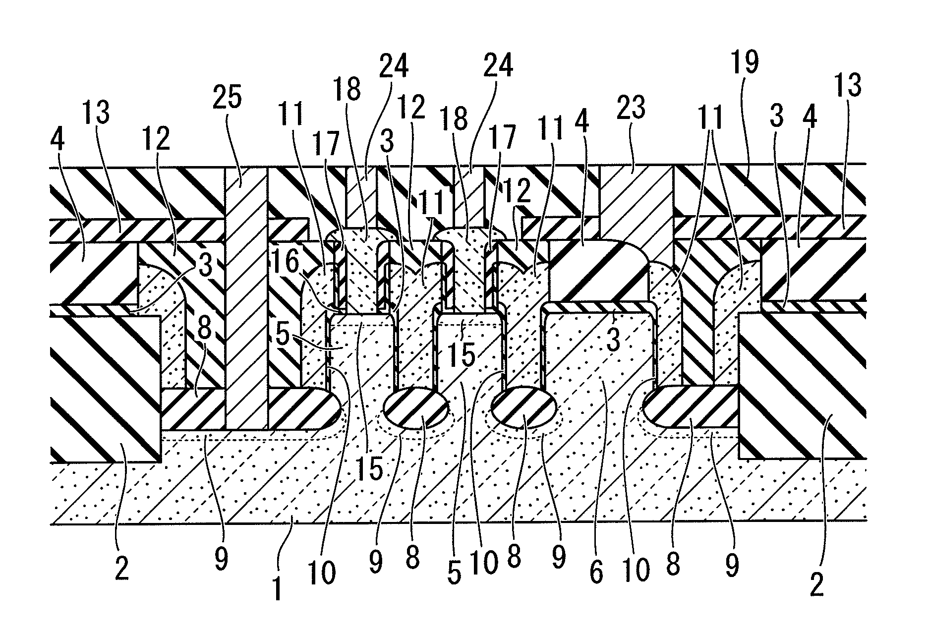
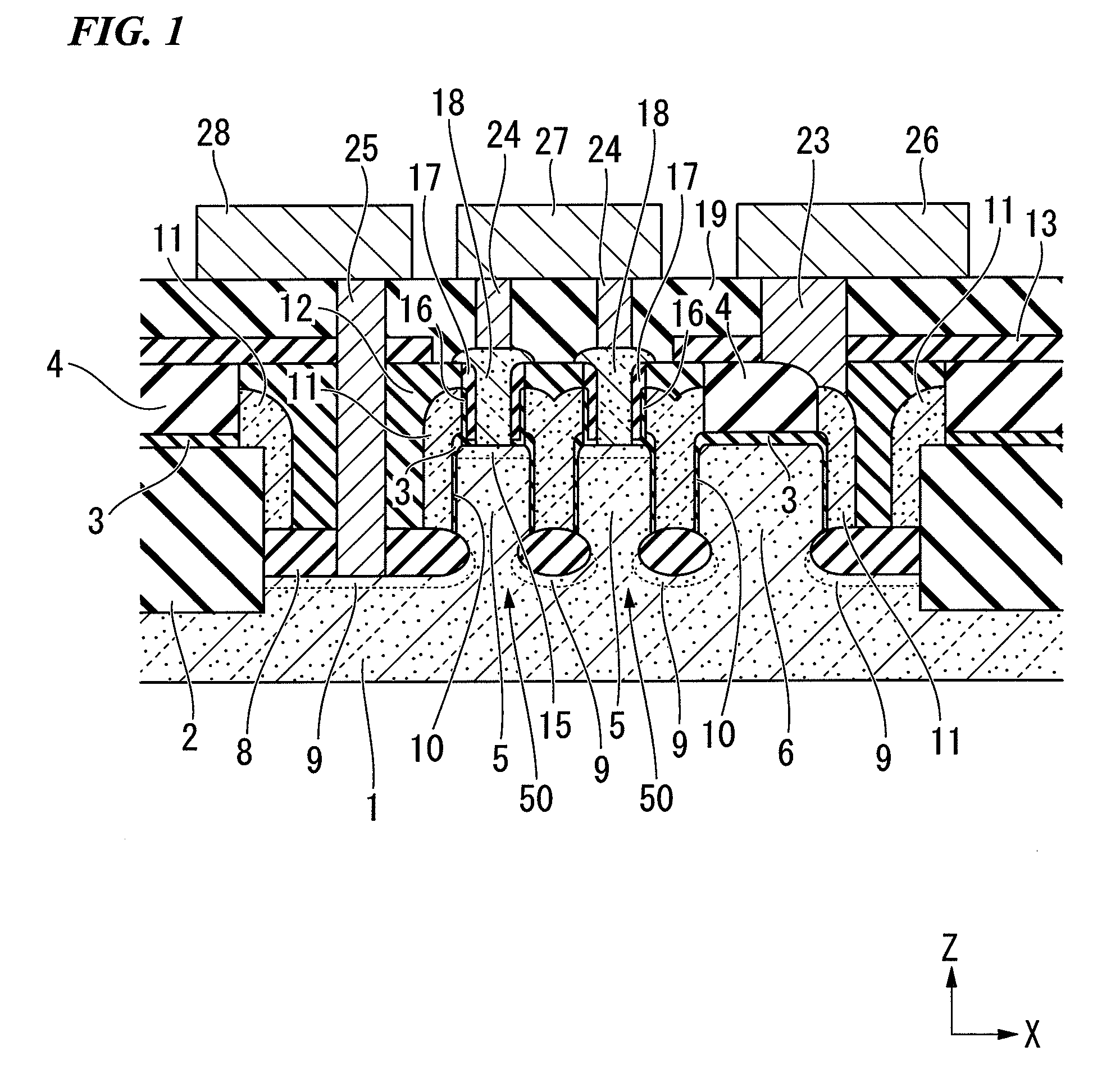
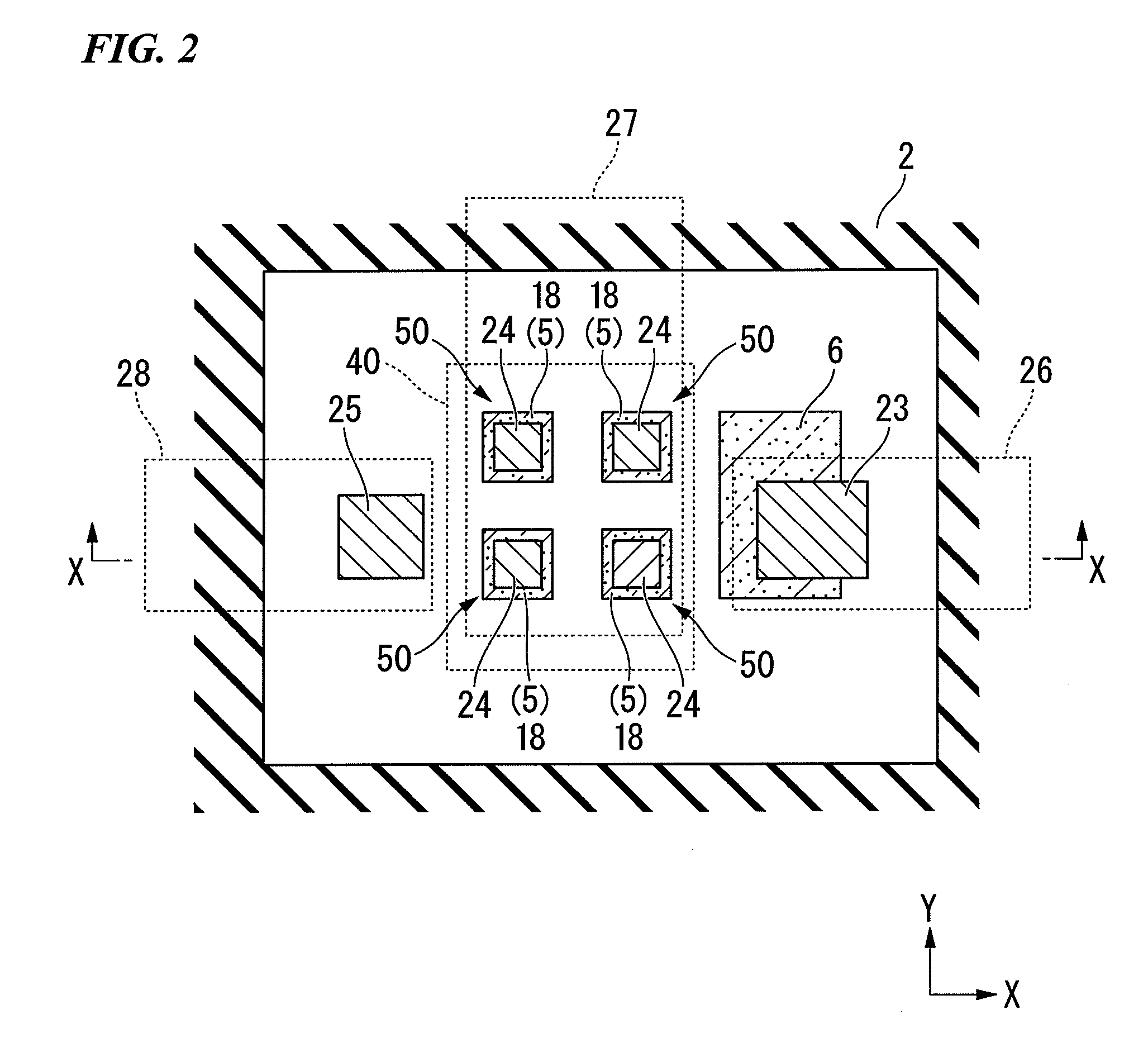
[0024]The invention will be now described herein with reference to illustrative embodiments. Those skilled in the art will recognize that many alternative embodiments can be accomplished using the teachings of the present invention and that the invention is not limited to the embodiments illustrated for explanatory purposes.
[0025]In the drawings mentioned in the following description, structural elements are illustrated so as to facilitate the understanding of the respective structural elements. As a result, scales of the illustrated structural elements and the number thereof may be different from those of actual structural elements. Moreover, the arrangement of the respective structural elements will be explained using an XYZ coordinate system. In this coordinate system, the Z direction is a direction orthogonal to a surface of a silicon substrate, the X direction and the Y direction are directions orthogonal to the Z direction, and the X direction and the Y direction are orthogona...
PUM
 Abstract
Description
Claims
Application Information