Stack-type semiconductor package

a semiconductor and stack technology, applied in semiconductor devices, semiconductor/solid-state device details, electrical apparatus, etc., can solve the problems of complex stack technology used for high-integration of semiconductor chips, laborious research into flip-chip packages, wafer-level packages, etc., to reduce production time and cost, reduce the number of process operations, and simplify the fabrication process

Inactive Publication Date: 2009-04-02
SAMSUNG ELECTRONICS CO LTD
View PDF2 Cites 25 Cited by
  • Summary
  • Abstract
  • Description
  • Claims
  • Application Information

AI Technical Summary

Benefits of technology

[0007]The present invention provides a stack-type semiconductor package and a method of fabricating the same, wherein signal transmission members are formed on a wafer level at one time to simplify the fabrication process and lessen the number of process operations, thereby reducing the production time and cost. The stack-type semiconductor package may also have improved reliability and improved structural solidity and productivity.

Problems solved by technology

Meanwhile, owing to the downscaling of electronic devices, semiconductor packages used for the electronic devices are showing the same tendency to become downscaled.
In recent years, laborious research into flip-chip packages, wafer-level packages, and wafer-level stack packages has progressed centering on miniaturization of these semiconductor packages.
In particular, the stack technology used for highly integrating a plurality of semiconductor chips has become complicated and the number of process operations has been greatly increased.

Method used


Image

  • Stack-type semiconductor package
  • Stack-type semiconductor package
  • Stack-type semiconductor package

Examples


Embodiment Construction

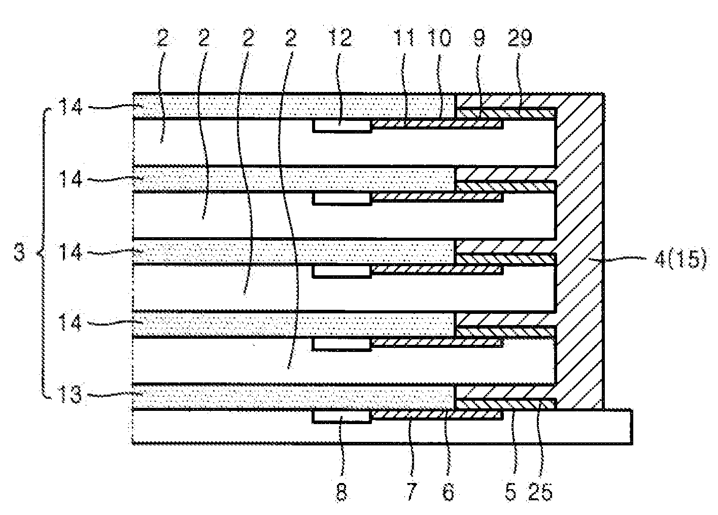
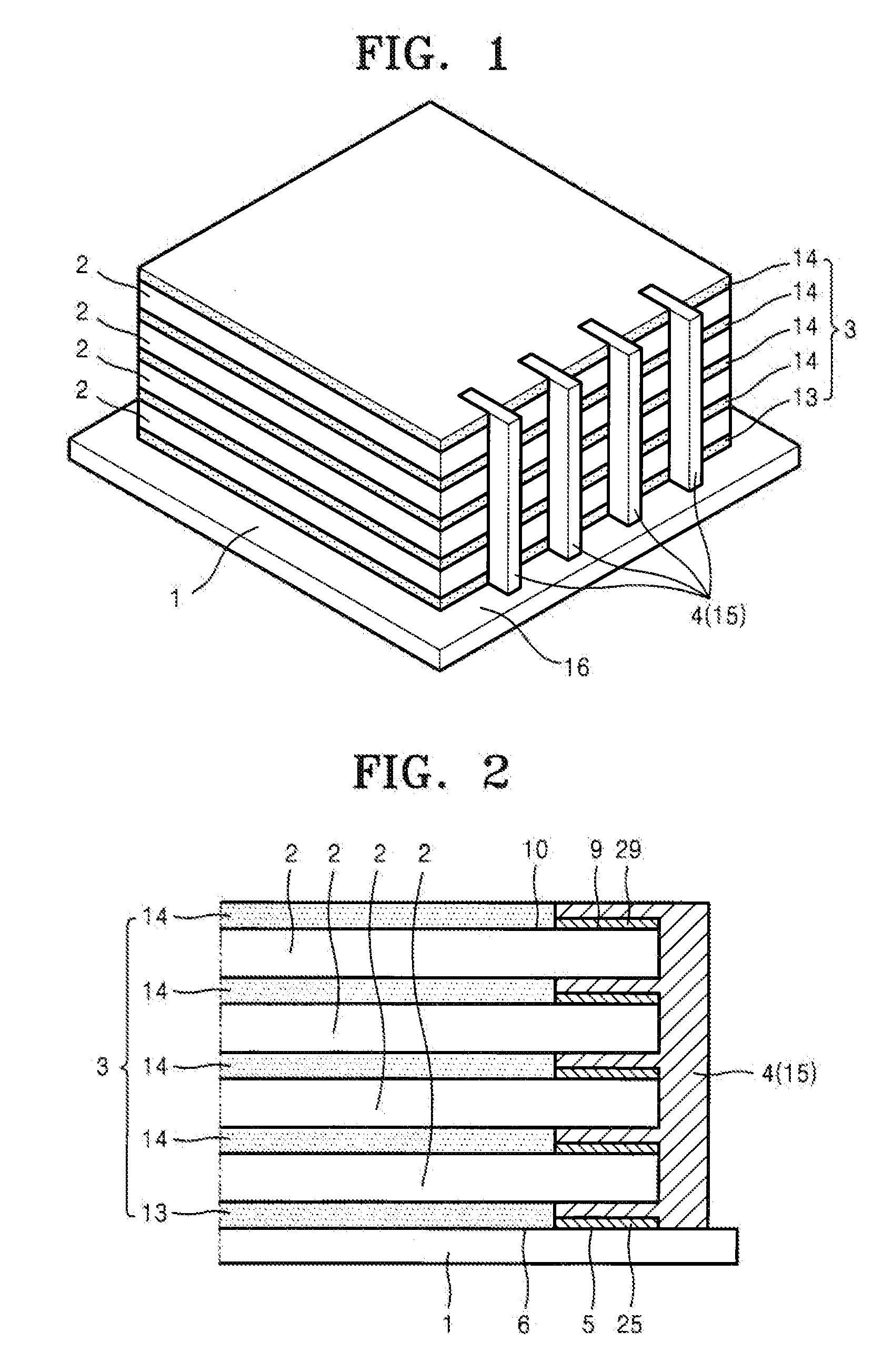
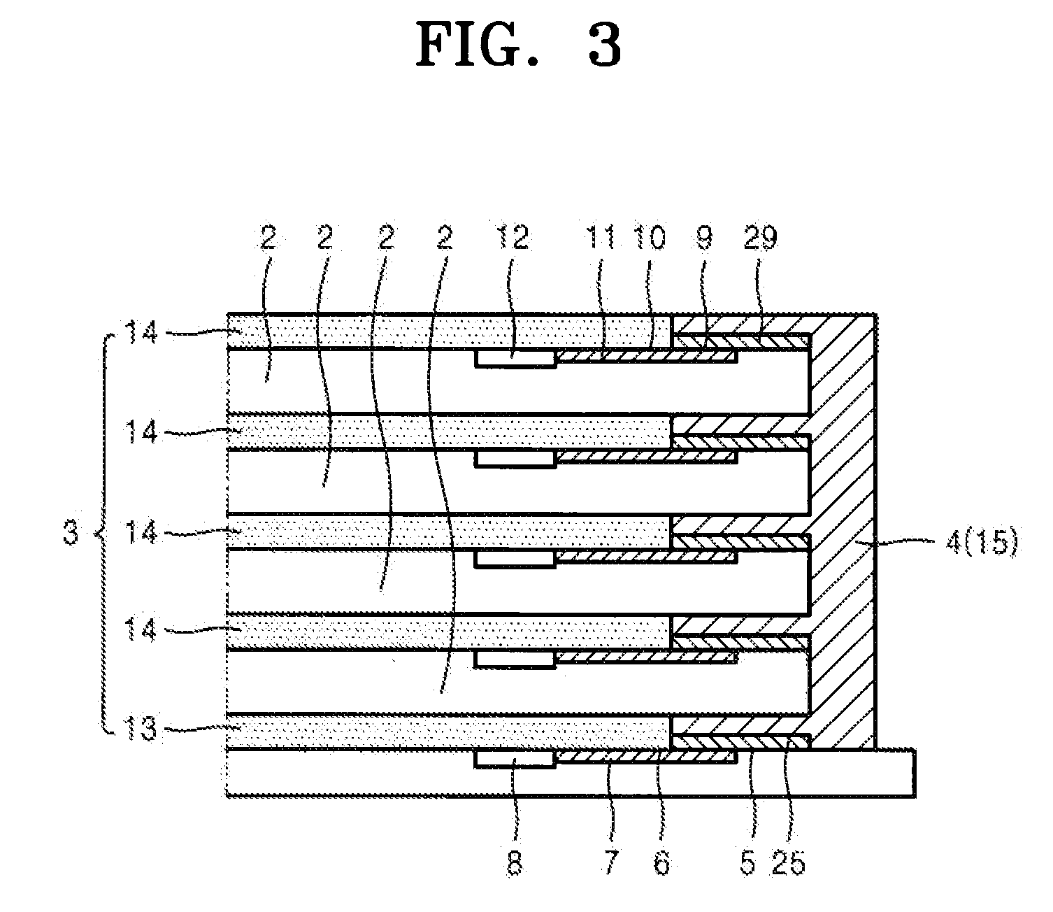
[0022]FIG. 1 is a perspective view of a stack-type semiconductor package according to an embodiment of the present invention. FIG. 2 is a cross-sectional view of the stack-type semiconductor package shown in FIG. 1.

[0023]Referring to FIGS. 1 and 2, a stack-type semiconductor package according to an embodiment of the present invention may include a base chip 1, at least one stack chip 2, an adhesive 3 substantially covering a top surface of each of the base chip 1 and the stack chips 2, and signal transmission members 4 for electrically connecting the base chip 1 and the stack chips 2.

[0024]Specifically, a circuit may be formed on one side of the base chip 1. Referring to FIG. 2, the circuit of the base chip 1 may include a base edge terminal 5 that extends to the signal transmission members 4 through a base edge terminal metal seed layer 25.

[0025]In this case, the base edge terminal 5 may not necessarily extend to the edge of the base chip 1. Thus, any kind of terminal that can exte...


PUM


Abstract

Provided is a stack-type semiconductor package including a base chip having a circuit formed on one of its surfaces, at least one stack chip having a circuit stacked on the base chip, an adhesive interposed between the base chip and the stack chip, and signal transmission members formed along a lateral surface of the stack chip. The fabrication process of this stack-type semiconductor package may be simplified and the number of process operations may be lessened, thereby reducing the production time and cost. Also, a state of electrical contact of a terminal with a signal transmission member may be solidified, thereby improving the reliability of the stack-type semiconductor package. Furthermore, new post-type signal transmission members are adopted instead of wires or electrodes so that the structural stability and productivity of the stack-type semiconductor package may be markedly enhanced.

Description

CROSS-REFERENCE TO RELATED PATENT APPLICATION[0001]This application claims the benefit of Korean Patent Application No. 10-2007-0099243, filed on Oct. 2, 2007, in the Korean Intellectual Property Office, the disclosure of which is incorporated herein in its entirety by reference.BACKGROUND OF THE INVENTION[0002]1. Field of the Invention[0003]The present invention relates to a stack-type semiconductor package, and more particularly, to a stack-type semiconductor package in which a stack chip is stacked on a wafer for forming a base chip and signal transmission members are formed on a wafer level at one time, thereby simplifying a fabrication process and reducing the number of process operations.[0004]2. Description of the Related Art[0005]In general, packaging processes for semiconductor chips with microcircuits use a plastic resin or ceramic to encapsulate the semiconductor chip in part to protect the chips and microcircuits from outer environmental elements. In addition, these pack...

Claims


Application Information

Patent Timeline
Patent Type & Authority Applications(United States)
IPC IPC(8): H01L23/538H01L21/58
CPCH01L21/561H01L23/3121H01L2224/29101H01L2924/014H01L2924/01033H01L2924/01006H01L24/24H01L24/29H01L24/82H01L24/97H01L25/0657H01L25/50H01L2224/24145H01L2224/97H01L2225/06541H01L2225/06551H01L2225/06575H01L2924/01047H01L2924/01078H01L2224/9202H01L2924/01005H01L2224/82H01L2924/00H01L23/12
Inventor CHOI, JU-ILCHUNG, HYUN-SOOLEE, IN-YOUNGLEE, HO-JINHWANG, SON-KWAN
Owner SAMSUNG ELECTRONICS CO LTD
Why Eureka
Try Eureka