Piezoelectric devices and methods for manufacturing same

a technology of piezoelectric devices and manufacturing methods, applied in the field of piezoelectric devices, can solve the problems of difficult mass production (with consequent item cost reduction) and achieve the effects of improving the electrical conductivity of wires, superior electrical conductivity, and increasing the affinity of wires

Inactive Publication Date: 2009-04-02
NIHON DEMPA KOGYO CO LTD
View PDF4 Cites 6 Cited by
  • Summary
  • Abstract
  • Description
  • Claims
  • Application Information

AI Technical Summary

Benefits of technology

[0010]The metal wires can be made of any of various suitable metals such as, but not limited to, iron (Fe), copper (Cu), nickel (Ni), stainless (SUS), or kovar alloy. These metals are relatively inexpensive and have superior electrical conductivity. The wires desirably are coated with a metal such as gold (Au). The gold layer on the metal wires increases the affinity of the wires to glass and improves the electrical conductivity of the wires through the glass base. Gold also improves connection of the wires to the respective connection electrodes. The surface roughness of the wires can be increased to increase the affinity of the wires to the glass of the base. The gold layer can be formed after increasing the surface roughness of the wires.
[0011]According to another aspect, methods for manufacturing piezoelectric devices are provided. An embodiment of such a method comprises preparing a lid wafer on which is formed an array of multiple lids, preparing a piezoelectric wafer on which is formed an array of multiple piezoelectric vibrating pieces each having a first electrode and a second electrode, and preparing a glass base wafer on which is defined an array of multiple bases. The glass base wafer has a first surface and an opposing second surface. Each base includes at least a first metal wire and a second metal wire extending through the base and having respective ends denuded to the first surface. The method includes the step of sandwiching the piezoelectric wafer between the lid wafer and the glass base wafer in a manner resulting in registration of each piezoelectric vibrating piece with a respective base and a respective lid. The wafers are bonded together in a manner resulting in bonding each of the piezoelectric vibrating pieces to a respective lid and respective base, and automatic connection of the denuded metal wire-ends on the first surface of the base to the first and second electrode patterns of the piezoelectric vibrating piece. The resulting multiple piezoelectric devices are then cut or otherwise detached from the bonded three-layered wafer. According to this method embodiment, assembly and sealing of individual piezoelectric devices as performed in conventional methods are avoided because multiple piezoelectric devices are made simultaneously by performing all process steps at the wafer level. This allows piezoelectric devices to be manufactured at lower cost than conventionally.
[0012]In the method, the step of preparing the glass base wafer can include the steps of arranging the first and second metal wires substantially parallel to each other at a designated spacing in a mold; fusing glass fragments at a fusing temperature of 900 C or less; forming a glass block containing the first and second metal wires by pouring the fused glass into the mold around the wires and allowing the glass to harden; and slicing the glass block in a direction perpendicular to the metal wires to form glass wafers. By forming glass wafers in this manner, each having embedded wires, mass production of bases can be achieved. Bubbles in the glass of the glass block can be reduced by pouring the fused glass into the mold after fusing the glass fragments.
[0013]In an alternative embodiment, the step of preparing the glass base wafer can further comprise the steps of placing the glass fragments along with arranged wires (sufficient to provide at least first and second metal wires for each base), arranged substantially parallel to each other in a designated space in a mold; fusing the glass fragments in the mold at 900 C or less to form a glass block containing the metal wires; allowing the fused glass to harden to form a glass block; and slicing the glass block in a direction perpendicular to the metal wires to form glass wafers. Thus, this embodiment differs from the first method embodiment by forming a glass block, containing the metal wires, in the mold by pouring the glass fragments (rather than a glass melt) into the mold and heating the mold to a fusing temperature. The glass wafers are manufactured by slicing them from the block so that mass production of glass wafers can be achieved.
[0014]If desired, a glass film can be formed on the surfaces of the metal wires to confer high affinity of the wires to the fused glass. After forming the glass film on the wires, the wires are arranged in the mold at designated positions. Thus, the first and second metal wires for each piezoelectric device formed from the glass wafer are strongly bonded to their respective glass base. This allows bonding of the wafers to be performed in a vacuum so as to seal a vacuum environment inside each piezoelectric device. Maintenance of the vacuum is assured due to the absence of any space between the first and second wires and the glass base of each piezoelectric device.
[0015]As noted above, the surface roughness of the metal wires can be increased to increase the affinity of the wires to the fused glass. The roughened wires are arranged at their designated positions in the mold. The consequent strong bonding of the first and second metal wires to the respective bases allows processing in a vacuum to produce a vacuum environment inside each piezoelectric device.

Problems solved by technology

Hence, mass-production (with consequent item cost reduction) is difficult.

Method used


Image

  • Piezoelectric devices and methods for manufacturing same
  • Piezoelectric devices and methods for manufacturing same
  • Piezoelectric devices and methods for manufacturing same

Examples


first embodiment

of Crystal Unit

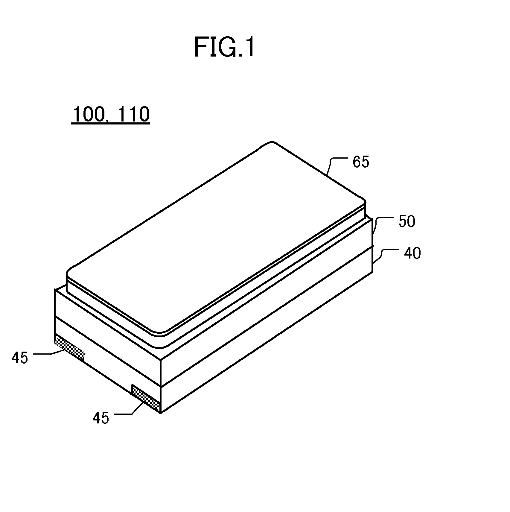
[0057]A crystal unit 100 (as an exemplary piezoelectric device) according to this embodiment is shown in FIGS. 4A-4D, which are schematic views. FIG. 4A is an elevational section along the line X-X in FIG. 4C, FIG. 4B is a plan view of the under (inner) surface of the lid 65 of the package, FIG. 4C is a top (plan) view of the crystal frame 50, and FIG. 4D is a top (plan) view of the first base 40.

[0058]In FIG. 4A the crystal unit 100 includes a crystal frame 50 in which a tuning-fork type crystal vibrating piece 30 is situated centrally. A first base 40 is attached to the bottom surface of the crystal frame 50, and a first lid 65 is attached to the top surface of the crystal frame 50. In the crystal frame 50 the tuning-fork type crystal vibrating piece 30 was formed from a crystal wafer 10 by etching.

[0059]As FIG. 4B shows, the lid 65 has a lid concave portion 67 formed by etching of the surface of the first lid on the crystal-frame side thereof. The first lid 65 can ...

second embodiment

of Crystal Unit

[0069]A crystal unit 110 according to this embodiment is described with reference to the schematic views shown in FIGS. 5A-5D. FIG. 5A is an elevational section along the line X-X in FIG. 5C, FIG. 5B is a plan view of the lower (inner) surface of the second lid 65′, FIG. 5C is a top plan view of the crystal frame 50, and FIG. 5D is a top view of the second base 40′.

[0070]In FIG. 5A the crystal unit 110 comprises a crystal frame 50 of which a tuning-fork type crystal vibrating piece 30 is a central portion. A second base 40′ is attached to the lower surface of the crystal frame 50 and a second lid 65′ is attached to the upper surface of the crystal frame 50.

[0071]Turning to FIG. 5B, the second lid 65′ includes a lid concave portion 67′ formed on the under-surface thereof. This under-surface will be situated inside the completed package. The lid concave portion 67′ is formed by etching of the lid material to a defined depth. The under-surface of the second lid 65′ also ...


PUM

PropertyMeasurementUnit
thicknessaaaaaaaaaa
lengthaaaaaaaaaa
widthaaaaaaaaaa

Abstract

Devices are disclosed that include a piezoelectric vibrating piece; a glass base and lid form a package enclosing the piezoelectric vibrating piece. The piece has first and second electrodes. The base has first and second opposing surfaces. The base mounts the piezoelectric vibrating piece, and the lid seals the piezoelectric vibrating piece in the package. The base includes first and second metal wires, extending therethrough, whose ends are denuded to the first and second surfaces and connected to the first and second electrodes, respectively. In disclosed methods for making the packaged devices, such as piezoelectric oscillators, multiple packaged devices are made simultaneously by stacking and simultaneously bonding respective wafers on which glass bases, piezoelectric vibrating pieces, and lids have been formed.

Description

CROSS-REFERENCE TO RELATED PATENT APPLICATION[0001]This application claims priority to, and the benefit of, Japan Patent Application No. 2007-251821, filed on Sep. 27, 2007, in the Japan Patent Office, the disclosure of which is incorporated herein by reference in its entirety.FIELD[0002]This disclosure relates to, inter alia, piezoelectric devices of which the package is formed from a glass wafer with embedded metal wires. The disclosure also pertains to methods for manufacturing piezoelectric devices, including sealing of piezoelectric vibrating pieces in their respective packages.DESCRIPTION OF THE RELATED ART[0003]With the progress of miniaturization and / or increases in the operating frequency of mobile communication apparatus and office automation (OA) equipment, piezoelectric oscillators used in this equipment must be progressively smaller and / or operate at higher frequency. Also required are piezoelectric oscillators that can be surface mounted on circuit boards.[0004]Contemp...

Claims


Application Information

Patent Timeline
Patent Type & Authority Applications(United States)
IPC IPC(8): H01L41/04H01L41/047H01L41/053H01L41/22H01L23/08H03H3/02H03H9/02
CPCH01L41/053H03H9/0595H03H9/1035H01L41/23Y10T29/42H01L2224/45147H01L2224/43848H01L2924/00H01L2924/00011H01L2924/01005
Inventor ONO, KOZOINOUE, TAKAHIRO
Owner NIHON DEMPA KOGYO CO LTD
Why Eureka
Try Eureka