Method and system for split voltage domain transmitter circuits

a transmitter circuit and split voltage technology, applied in the field of integrated circuit power control, can solve problems such as excessive leakage, degrade performance, and drive gate voltages lower

Active Publication Date: 2009-04-02
CISCO TECH INC
View PDF10 Cites 10 Cited by
  • Summary
  • Abstract
  • Description
  • Claims
  • Application Information

AI Technical Summary

Benefits of technology

[0018]FIG. 1D is a block diagram of an exemplary n-type field effect transistor circuit, in accordance with an embodiment of the inventi...

Problems solved by technology

Furthermore, as device sizes continue to shrink for higher speed and lower power consumption, a high voltage may degrade performance and cause excessive leakage.
With thinner gate oxides, gate leakage current may become significant using historical bi...

Method used


Image

  • Method and system for split voltage domain transmitter circuits
  • Method and system for split voltage domain transmitter circuits
  • Method and system for split voltage domain transmitter circuits

Examples


Embodiment Construction

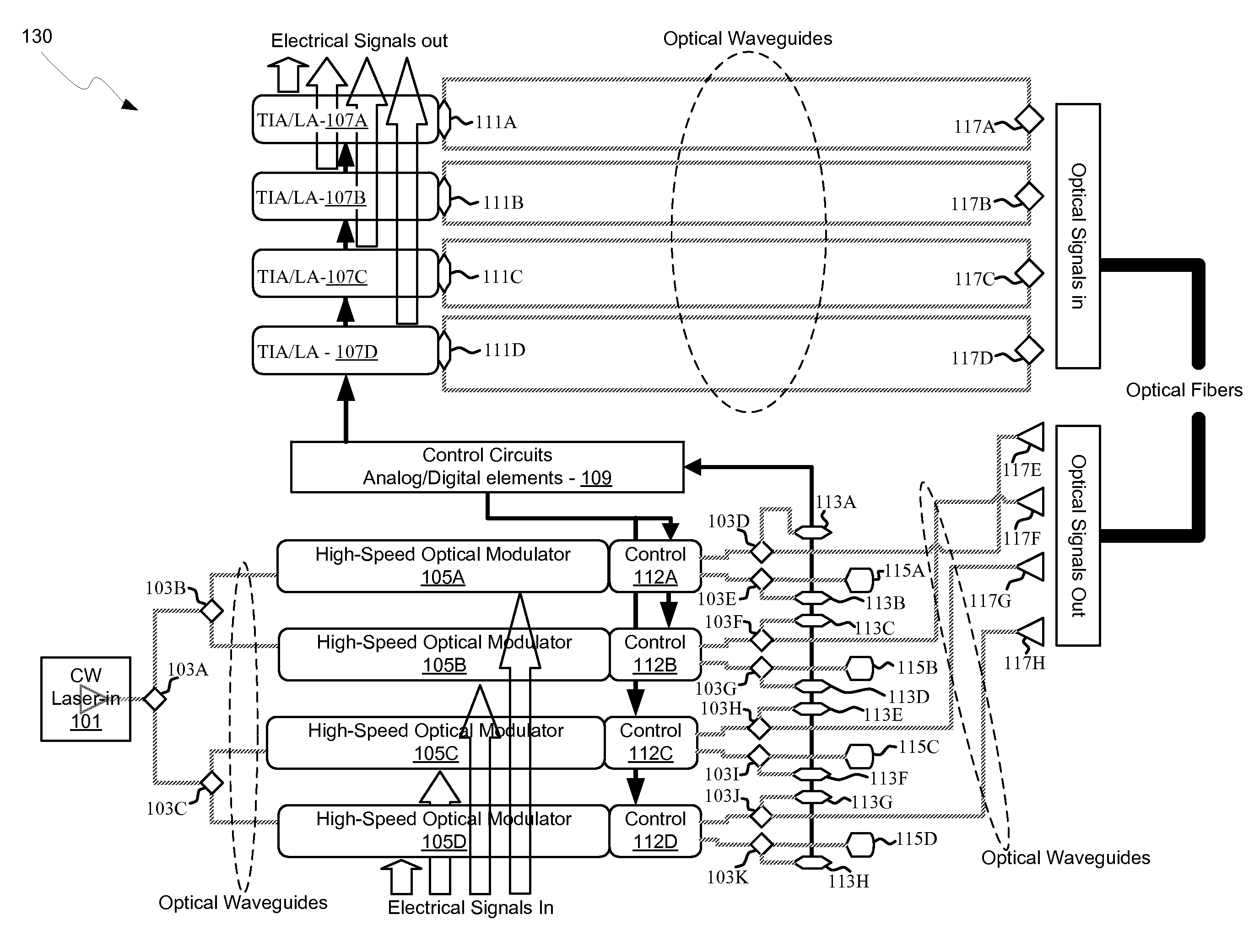
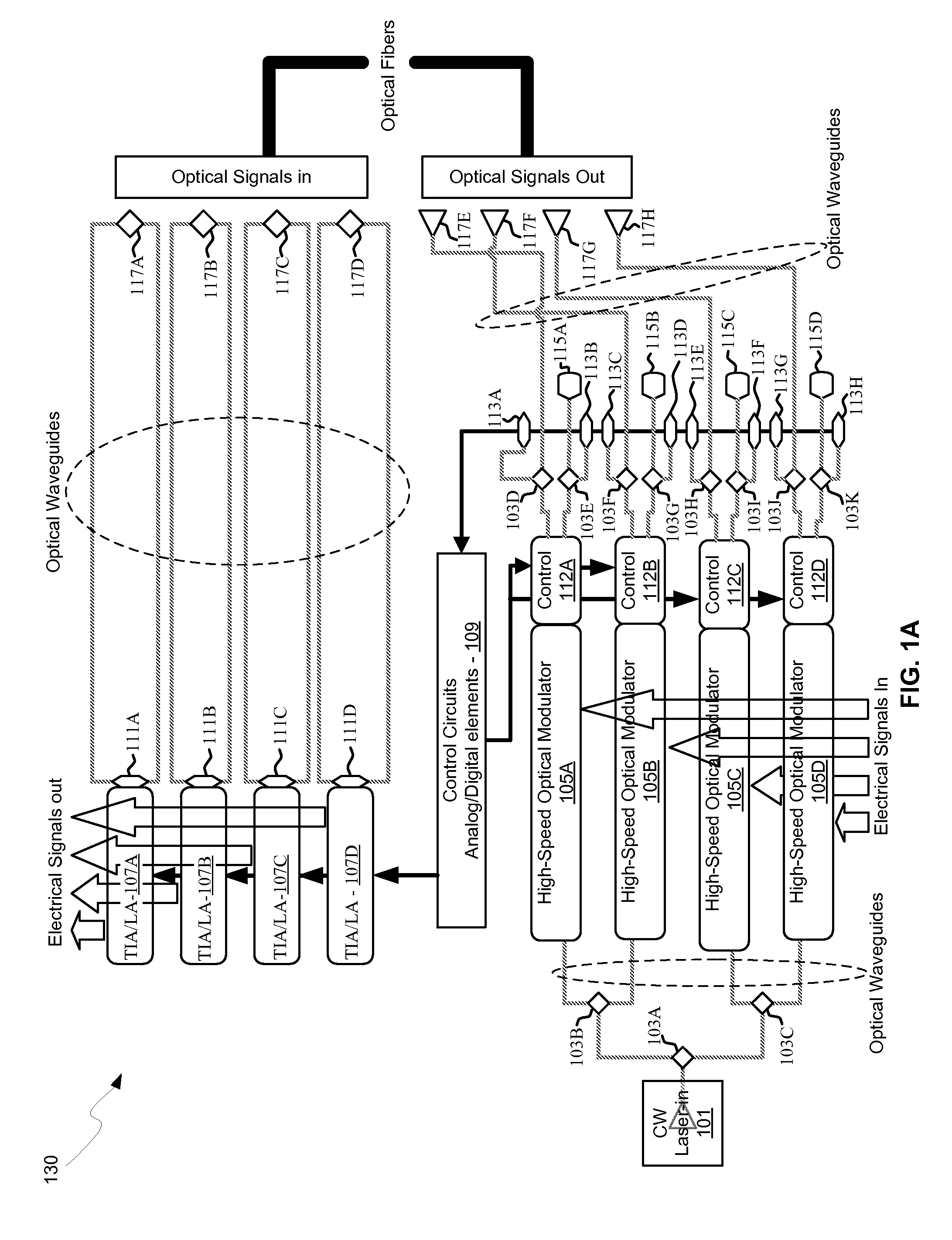
[0025]Certain aspects of the invention may be found in a method and system for split voltage domain transmitter circuits. Exemplary aspects of the invention may comprise amplifying a received signal in a plurality of partial voltage domains. Each of the partial voltage domains may be offset by a DC voltage from the other partial voltage domains. A sum of the plurality of partial domains may be equal to a supply voltage of the integrated circuit. A series of diodes may be driven in differential mode via the amplified signals. An optical signal may be modulated via the diodes, which may be integrated in a Mach-Zehnder modulator or a ring modulator, for example. The diodes may be connected in a distributed configuration. The amplified signals may be communicated to the diodes via even-mode coupled transmission lines. The partial voltage domains may be generated via stacked source follower or emitter follower circuits. The voltage domain boundary value may be at one half the supply volt...


PUM


Abstract

Methods and systems for split voltage domain transmitter circuits are disclosed and may include amplifying a received signal in a plurality of partial voltage domains. Each of the partial voltage domains may be offset by a DC voltage from the other partial voltage domains. A sum of the plurality of partial domains may be equal to a supply voltage of the integrated circuit. A series of diodes may be driven in differential mode via the amplified signals. An optical signal may be modulated via the diodes, which may be integrated in a Mach-Zehnder or a ring modulator. The amplified signals may be communicated to the diodes, connected in a distributed configuration, via even-mode coupled transmission lines. The partial voltage domains may be generated via stacked source follower or emitter follower circuits. The voltage domain boundary value may be at one half the supply voltage due to symmetric stacked circuits.

Description

CROSS-REFERENCE TO RELATED APPLICATIONS / INCORPORATION BY REFERENCE[0001]This application makes reference to and claims priority to U.S. Provisional Application Ser. No. 60 / 997,282 filed on Oct. 2, 2007, which is hereby incorporated herein by reference in its entirety.[0002]This application also makes reference to:[0003]U.S. Pat. No. 7,039,258; and[0004]U.S. patent application Ser. No. ______ (Attorney Docket No. 19509US01) filed on even date herewith.[0005]Each of the above stated applications is hereby incorporated herein by reference in its entirety.FEDERALLY SPONSORED RESEARCH OR DEVELOPMENT[0006][Not Applicable]MICROFICHE / COPYRIGHT REFERENCE[0007][Not Applicable]FIELD OF THE INVENTION[0008]Certain embodiments of the invention relate to integrated circuit power control. More specifically, certain embodiments of the invention relate to a method and system for split voltage domain transmitter circuits.BACKGROUND OF THE INVENTION[0009]Electronic circuits typically require a bias vol...

Claims


Application Information

Patent Timeline
IPC IPC(8): H04B10/04
CPCG02B6/4201H04L25/0272H04B10/564H04B10/516H04B10/501G02B6/4242H04B10/60H04B10/693H04L25/061
Inventor WELCH, BRIANKUCHARSKI, DANIEL
Owner CISCO TECH INC
Why Eureka
Try Eureka