
Method of minimizing via sidewall damages during dual damascene trench reactive ion etching in a via first scheme

Inactive Publication Date: 2009-04-02
INFINEON TECH AG +2
View PDF16 Cites 19 Cited by
  • Summary
  • Abstract
  • Description
  • Claims
  • Application Information

AI Technical Summary

Benefits of technology

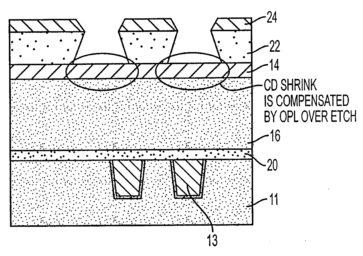
[0017]One aspect of the present invention is directed to a method of minimizing undercut of a hard mask in an integrated circuit (IC) structure including steps of providing an IC structure having a substrate, a interlayer dielectric layer, and a hard mask, forming a via in said IC structure, and depositing an organic planarizing layer (OPL) over the IC structure such that it fills the vias formed therein. The method also includes steps of forming a masking structure layer over the OPL, forming an opening in the masking structure that has a critical dimension (CD) smaller than an opening design dimension, anisotropic etching the OPL such that sidewall of the via remains covered with the OPL while forming a trench, and removing any remaining OPL on the sidewalls and trench, wherein the undercut of the sidewalls with respect to the hard mask is minimized by the covering of OPL during the anisotropic etching process.

Problems solved by technology

The complexity of this wiring becomes immediately appreciable once one realizes that there are usually hundreds of millions or more semiconductor devices (transistors in particular) formed on a single IC, and all these semiconductor devices need to be properly connected.
Microchip interconnect technology has become a critical challenge for future IC advancements due to the increasing difficulties to reduce signal propagation delay or interference caused by the increasingly dense interconnects.
The problem is particularly acute considering that while an increase of metallization density means longer signal delays caused by the interconnects, a corresponding increase of transistor density means shorter signal traveling time between local semiconductor devices, making metallization increasingly a bottleneck in enhancing IC performance.
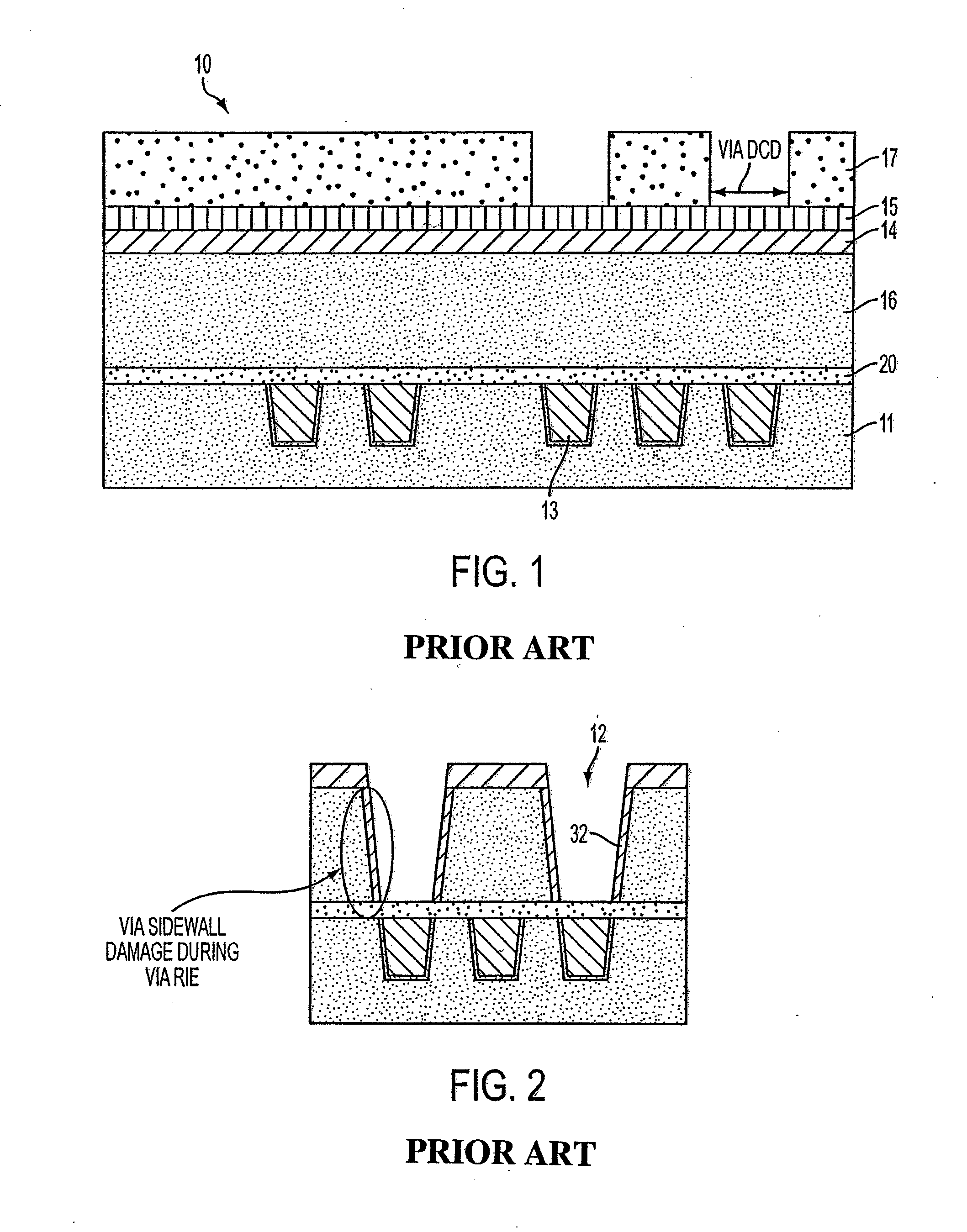
This step alone causes great damage to the sidewall 32.
Much of this undercut is the result of removal of carbon depletion layer by DHF clean which is actually caused by the etching processes and is particularly troublesome when in low-k and ultra low-k dielectric applications and results in an increase in dielectric constant in the IDL 16.
The undercut itself is a problem because it causes problem for the barrier layer deposition and hence prevents Cu from properly bonding to the via 12 sidewalls 32.
This improper bonding results in device reliability issues for devices manufactured using this process.

Method used


Image

  • Method of minimizing via sidewall damages during dual damascene trench reactive ion etching in a via first scheme
  • Method of minimizing via sidewall damages during dual damascene trench reactive ion etching in a via first scheme
  • Method of minimizing via sidewall damages during dual damascene trench reactive ion etching in a via first scheme

Examples


Embodiment Construction

[0044]As described above with reference to a known dual damascene process, via sidewalls are damaged during a via strip step, and then are further damaged by processing steps including the trench etch, etc. To minimize this damage, one aspect of the present invention is directed to a scheme which protects the sidewalls during the trench reactive ion etch (RIE) process, in a via first dual damascene process.

[0045]In one aspect of the present invention, an etch sequence is used on masking structure for example an oxide-like over-layer (OLO) and an OPL integration scheme where the via sidewalls closest to the trench are protected by the OPL during OPL etch, an oxide hard mask open and main etches to avoid any unnecessary exposure to the sidewalls. In addition it has been found that this process does not affect the CD of trench only structures, having no via sidewalls to be concerned with.

[0046]FIG. 8 shows a cross section of a portion of an IC 10 in which vias 12 have already been form...


PUM


Abstract

A method of minimizing undercut of a hard mask in an integrated circuit (IC) structure including steps of providing an IC structure having a substrate, a interlayer dielectric layer, and a hard mask, forming a via in said IC structure, and depositing an organic planarizing layer (OPL) over the IC structure such that it fills the vias formed therein. The method also includes steps of forming a masking structure layer over the OPL, forming an opening in the masking structure that has a critical dimension (CD) smaller than an opening design dimension, anisotropic etching the OPL such that sidewall of the via remains covered with the OPL while forming a trench, and removing any remaining OPL on the sidewalls and trench, wherein the undercut of the sidewalls with respect to the hard mask is minimized by the covering of OPL during the anisotropic etching process.

Description

BACKGROUND[0001]1. Field of the Invention[0002]The present invention relates generally to the field of semiconductors, particularly to manufacturing methods for fabricating semiconductor devices, and more particularly to the Back-End-Of-Line (BEOL) semiconductor manufacturing process using via first dual damascene processes.[0003]2. Description of the Prior Art[0004]The semiconductor manufacturing process, when likened to an assembly line, includes two major components, namely the Front-End-of-Line (FEOL) which includes the multilayer process of the actual forming of semiconductor devices (transistors, etc.) on a semiconductor substrate, and the Back-End-Of-Line (BEOL) which includes the metallization after the semiconductor devices have been formed. Like all electronic devices, semiconductor devices in a microchip such as an integrated circuit (IC) need to be electronically connected through wiring. In an integrated circuit, such wiring is done through multilayer metallization on t...

Claims


Application Information

Patent Timeline
IPC IPC(8): H01L21/311H01L21/44
CPCH01L21/02063H01L21/0337H01L21/0338H01L21/76816H01L21/31144H01L21/76808H01L21/76814H01L21/31116
Inventor SRIVASTAVA, RAVI PRAKASHWENDT, HERMANNKUMAR, KAUSHIK A.LEE, NICHOLSON M.
Owner INFINEON TECH AG
Learn More