Unit pixels, image sensor containing unit pixels, and method of fabricating unit pixels

a technology of image sensor and unit pixel, which is applied in the direction of electrical equipment, semiconductor devices, radio frequency control devices, etc., can solve the problem that light incident obliquely onto the microlens may not reach the photoelectric transformation element, and achieve the effect of improving photosensitivity and reducing loss of light inciden

Active Publication Date: 2009-04-09
SAMSUNG ELECTRONICS CO LTD
View PDF3 Cites 107 Cited by
  • Summary
  • Abstract
  • Description
  • Claims
  • Application Information

AI Technical Summary

Benefits of technology

[0010]Example embodiments provide unit pixels that may provide improved photosensitivity by reducing loss of light incident on a photoelectric transformation element.

Problems solved by technology

However, even with the use of a microlens within an image sensor for condensing light, light incident obliquely onto the microlens may not reach a photoelectric transformation element.

Method used


Image

  • Unit pixels, image sensor containing unit pixels, and method of fabricating unit pixels
  • Unit pixels, image sensor containing unit pixels, and method of fabricating unit pixels
  • Unit pixels, image sensor containing unit pixels, and method of fabricating unit pixels

Examples


Embodiment Construction

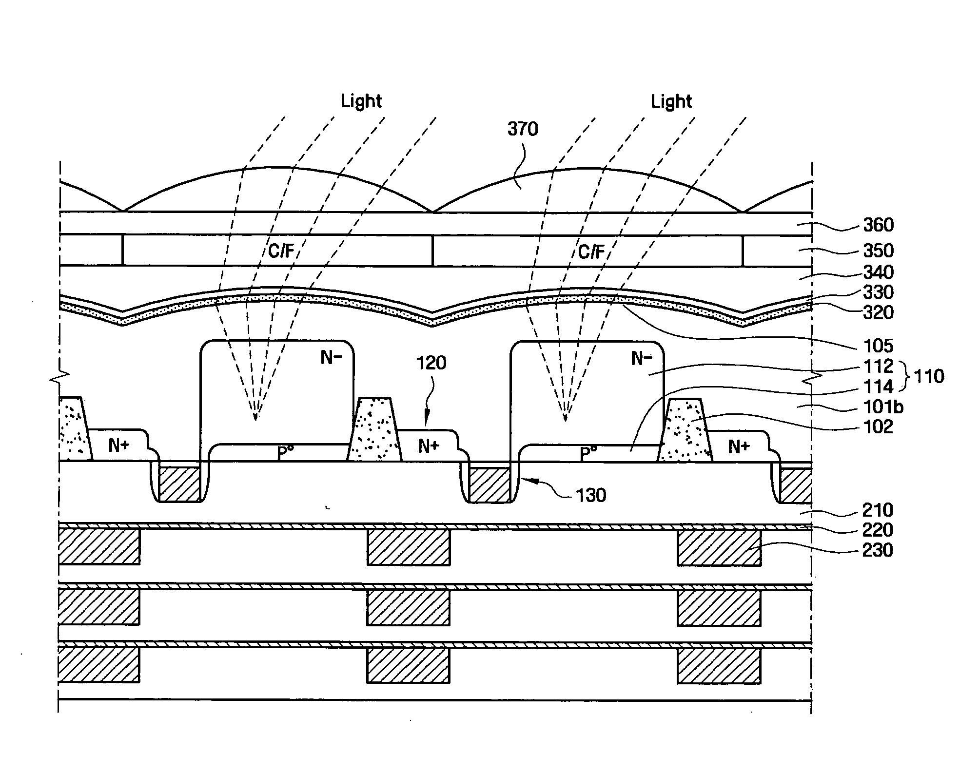
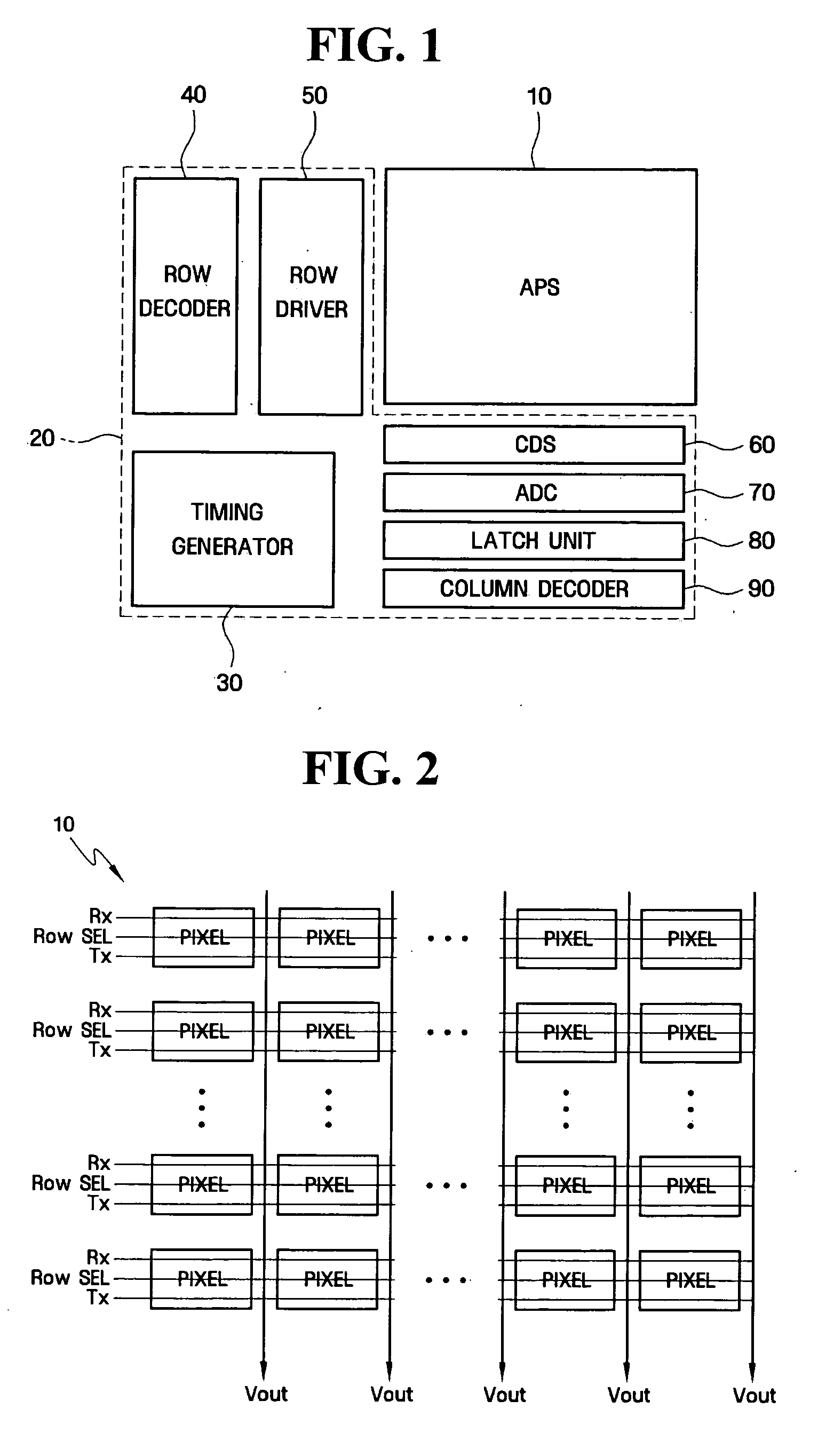
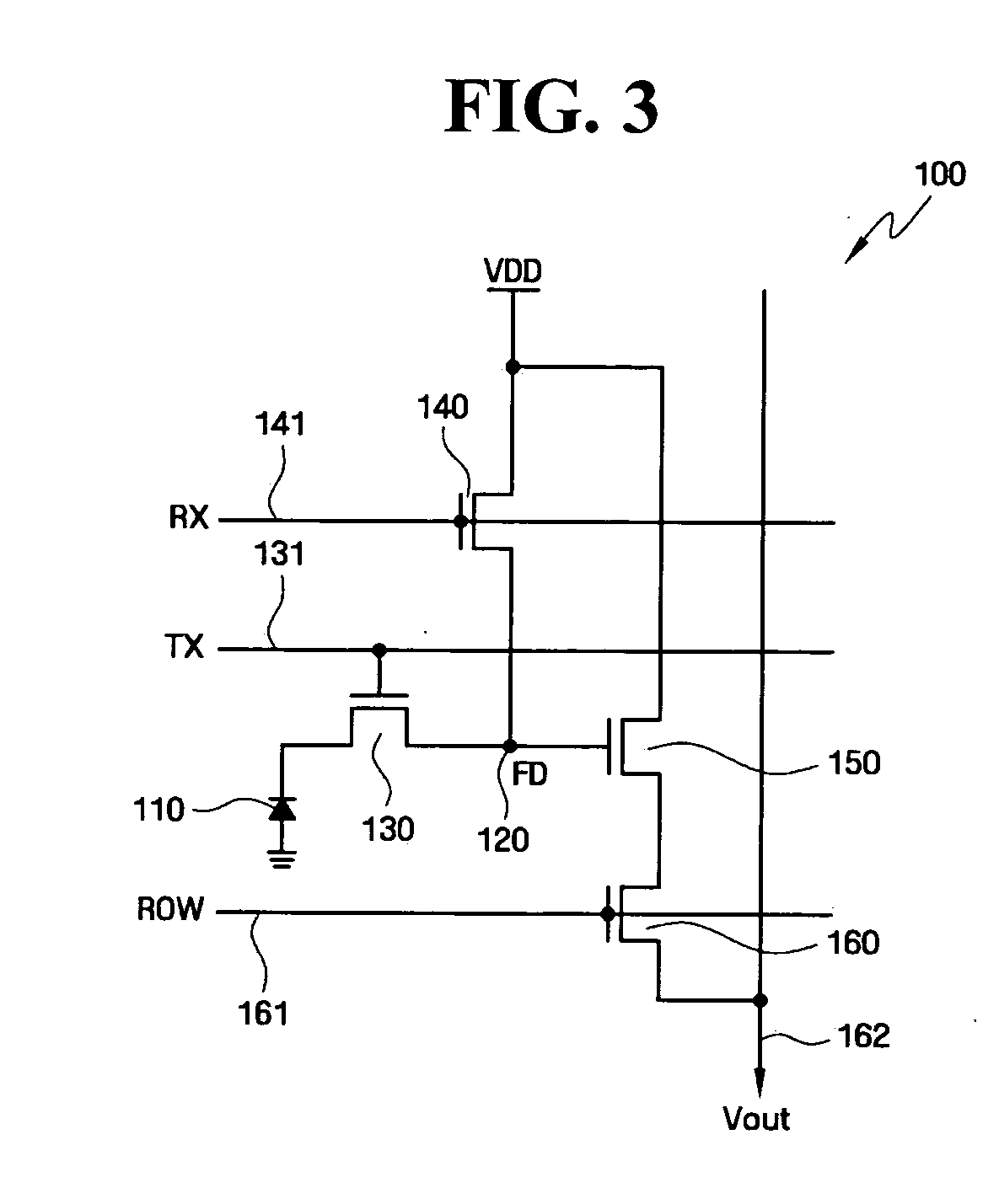
[0041]Detailed example embodiments are disclosed herein. However, specific structural and functional details disclosed herein are merely representative for purposes of describing example embodiments. Example embodiments may, however, be embodied in many alternate forms and should not be construed as limited to only the embodiments set forth herein.

[0042]Accordingly, while example embodiments are capable of various modifications and alternative forms, embodiments thereof are shown by way of example in the drawings and will herein be described in detail. It should be understood, however, that there is no intent to limit example embodiments to the particular forms disclosed, but to the contrary, example embodiments are to cover all modifications, equivalents, and alternatives falling within the scope of example embodiments. Like numbers refer to like elements throughout the description of the figures.

[0043]It will be understood that, although the terms first, second, etc. may be used h...


PUM


Abstract

Example embodiments provide a unit pixel, an image sensor containing unit pixels, and a method of fabricating unit pixels. The unit pixel may include a semiconductor substrate, photoelectric transducers formed within the semiconductor substrate, multi-layered wiring layers formed on a frontside of the semiconductor substrate, inner lenses formed on a backside of the semiconductor substrate corresponding to the photoelectric transducers, and microlenses formed above the inner lenses.

Description

[0001]This application claims priority under 35 U.S.C. §119 to Korean Patent Application No. 10-2007-0100459 filed on Oct. 5, 2007 in the Korean Intellectual Property Office, the entire contents of which are incorporated herein by reference.BACKGROUND[0002]1. Field[0003]Example embodiments are directed to unit pixels, an image sensor containing unit pixels, and method of fabricating unit pixels, and, more particularly, to unit pixels with improved photosensitivity, an image sensor containing unit pixels with improved photosensitivity, and a method of fabricating unit pixels with improved photosensitivity.[0004]2. Description of the Related Art[0005]Image sensors may be semiconductor elements that convert an optical image into an electrical signal. Image sensors may be categorized into charge coupled devices (CCDs) and complementary metal-oxide-semiconductor (CMOS) image sensors.[0006]A CCD may have a structure in which each MOS capacitor is more closely located and charges are store...

Claims


Application Information

Patent Timeline
Patent Type & Authority Applications(United States)
IPC IPC(8): H01L31/00H01L21/00
CPCH01L27/14627H01L27/1464H01L27/14685H01L27/146
Inventor PARK, BYUNG-JUN
Owner SAMSUNG ELECTRONICS CO LTD
Why Eureka
Try Eureka