Nonvolatile semiconductor memory device and manufacturing method therefor

a semiconductor memory and non-volatile technology, applied in the direction of semiconductor devices, electrical devices, transistors, etc., can solve the problems of extremely difficult to uniformly implant impurities in the depth direction, data write problems, etc., to achieve the effect of reducing the overlap area between the source diffusion layer and the floating gate, enhancing the coupling between the floating gate and the polysilicon plug, and reducing the cell size appropriately

Inactive Publication Date: 2009-04-16
RENESAS ELECTRONICS CORP
View PDF10 Cites 18 Cited by
  • Summary
  • Abstract
  • Description
  • Claims
  • Application Information

AI Technical Summary

Benefits of technology

[0023]According to the present invention, coupling between a floating gate and a polysilicon plug can be enhanced. As a result, an overlap area between a source diffusion layer and the floating gate can be reduced, and therefore a cell size can be appropriately reduced without forming a trench.

Problems solved by technology

The reduction of the overlap region may cause a problem in the data write.
For all of the memory cells, it is extremely difficult to uniformly implant the impurities in the depth direction.

Method used


Image

  • Nonvolatile semiconductor memory device and manufacturing method therefor
  • Nonvolatile semiconductor memory device and manufacturing method therefor
  • Nonvolatile semiconductor memory device and manufacturing method therefor

Examples


first embodiment

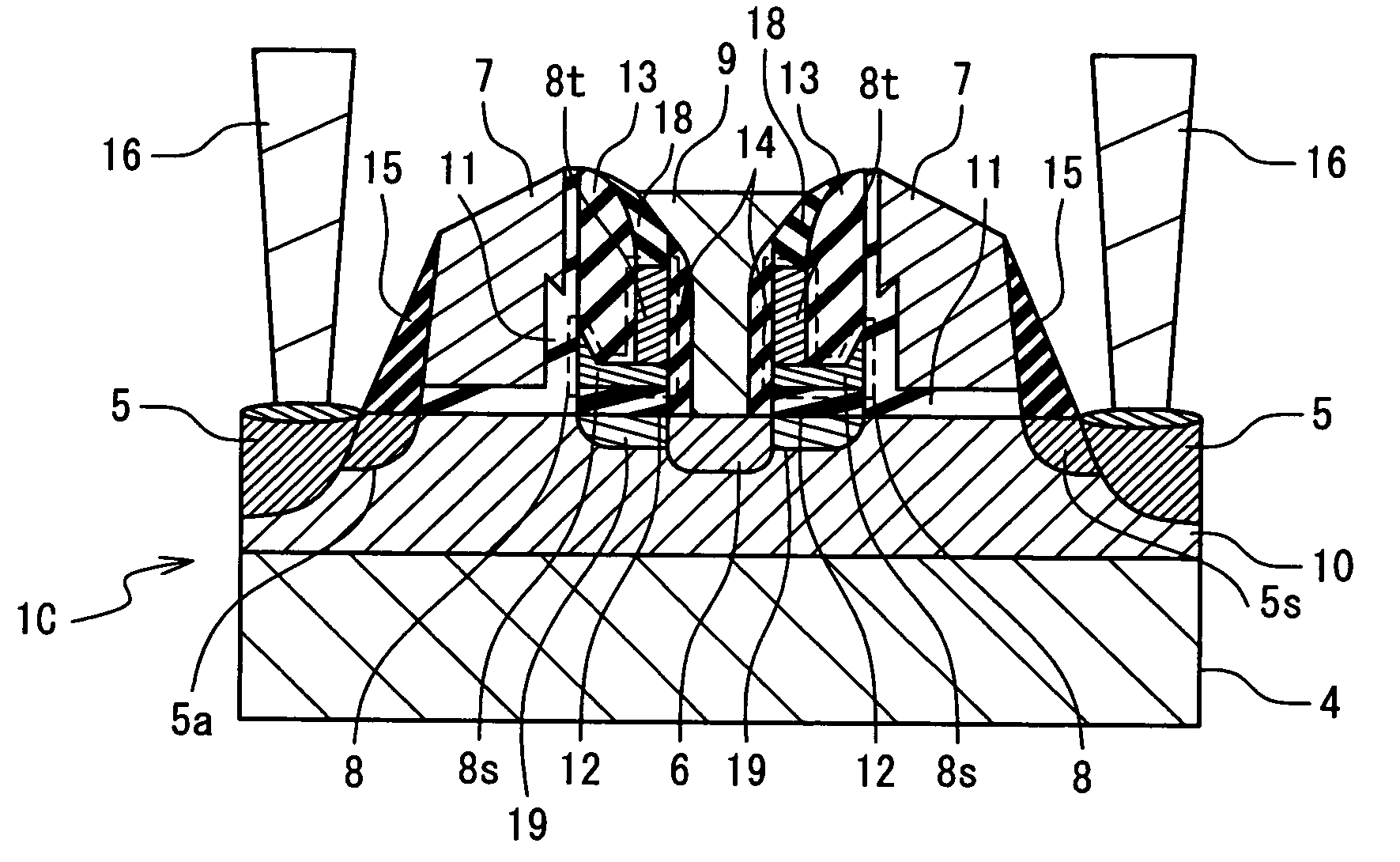
[0052]FIG. 4 is a cross-sectional view showing a configuration of a split gate type nonvolatile semiconductor memory device 1 as the nonvolatile semiconductor memory device according to a first embodiment of the present invention (hereinafter referred to as). In the split gate type nonvolatile semiconductor memory device 1 of the first embodiment, channel hot electrons generated in a substrate are injected to a floating gate in a write operation. Also, the electrons are drawn out from the floating gate to a control gate in an erase operation. Further, a read voltage is applied to the control gate to detect a state of a memory cell (ON or OFF).

[0053]Referring to FIG. 4, the split gate type nonvolatile semiconductor memory device 1 of the first embodiment contains first and second memory cells 1C which are formed symmetrically with respect to a plane. The first and second memory cells 1C are manufactured in a self-alignment manner. The nonvolatile semiconductor memory cells operate in...

second embodiment

[0090]The split gate type nonvolatile semiconductor memory device 1 according to a second embodiment of the present invention will be described below in detail with reference to the drawings. In the second embodiment, the second polysilicon films 27 are isolated in a manner different from that in the first embodiment. FIGS. 7A-1 to 7A-5 are diagrams showing the memory device 1 of the second embodiment in a first process for isolating the second polysilicon films 27.

[0091]FIG. 7A-5 is a plan view of the memory device 1 in the first process. FIG. 7A-1 is a cross-sectional view of the semiconductor memory device 1 along the line A-A in FIG. 7A-5, and FIG. 7A-2 is a cross-sectional view of the semiconductor memory device 1 along the line B-B in FIG. 7A-5. Also, FIG. 7A-3 is a cross-sectional view of the semiconductor memory device 1 along the line C-C in FIG. 7A-5, and FIG. 7A-4 is a cross-sectional view of the semiconductor memory device 1 along the line D-D in FIG. 7A-5.

[0092]In the f...

third embodiment

[0097]The split gate type nonvolatile semiconductor memory device 1 according to a third embodiment of the present invention will be described below with reference to the drawings. FIG. 8 is a cross-sectional view showing a structure of the split gate type nonvolatile semiconductor memory device 1 in the third embodiment of the present invention. In the first and second embodiments, the present invention is applied to the split gate type nonvolatile semiconductor memory device 1 to be manufactured in a self-alignment. In the third embodiment, the present invention is applied to the split gate type nonvolatile semiconductor memory device 1 to be manufactured without use of the self-alignment. As shown in FIG. 8, the split gate type nonvolatile semiconductor memory device 1 in the third embodiment is provided with the control gate 7 formed to cover the floating gate 8. The control gate 7 and the floating gate 8 are electrically insulated from each other by an interlayer insulating fil...


PUM


Abstract

In a nonvolatile semiconductor memory device, a floating gate is formed on a semiconductor substrate through a gate insulating film, and has a first portion contacting the gate insulating film and a second portion extending upwardly from a part of a surface of the first portion. A first diffusion layer is formed in the semiconductor substrate to have a plane parallel to a surface of the semiconductor substrate. A second diffusion layer is formed in the semiconductor substrate, to have the plane. A control gate is provided near the floating gate above a channel region in the semiconductor substrate and is formed on a first side of the first portion. A conductive film is connected with the first diffusion layer and is formed on a second side of the first portion and a first side of the second portion through the first insulating film.

Description

INCORPORATION BY REFERENCE[0001]This Patent Application claims priority on convention based on Japanese Patent Application No. 2007-268005. The disclosure thereof is incorporated herein by reference.BACKGROUND OF THE INVENTION[0002]1. Field of the Invention[0003]The present invention relates to a nonvolatile semiconductor memory device and a manufacturing method therefor.[0004]2. Description of Related Art[0005]As a nonvolatile semiconductor memory device in that a storage content is not erased even if power is turned off, a split gate type nonvolatile semiconductor memory device is known, as described in U.S. Pat. No. 6,525,371 B2. FIG. 1 is a cross-sectional view illustrating a configuration of the split gate type nonvolatile semiconductor memory device described in the above U.S. Pat. No. 6,525,371 B2. In this split gate type nonvolatile semiconductor memory device, a plurality of memory elements (hereinafter to be referred to as split gate type nonvolatile semiconductor memory c...

Claims


Application Information

Patent Timeline
Patent Type & Authority Applications(United States)
IPC IPC(8): H01L29/788H01L21/336
CPCH01L27/115H01L29/7881H01L29/42324H01L27/11521H10B69/00H10B41/30
Inventor IO, EIJI
Owner RENESAS ELECTRONICS CORP
Why Eureka
Try Eureka