MRAM with means of controlling magnetic anisotropy

Active Publication Date: 2009-04-16
TAIWAN SEMICON MFG CO LTD
View PDF20 Cites 60 Cited by
  • Summary
  • Abstract
  • Description
  • Claims
  • Application Information

AI Technical Summary

Benefits of technology

[0027]A second object of the present invention is to provide such a device in which the effects of shape anisotropy, and stress and magnetostriction induced anisotropy are combined to produce a switching field, Hs that minimizes the effects of thermal agitation.
[0028]These objects will be met by a MRAM spin transfer device design in which a significant portion of free layer magnetic anisotropy will be provided by stress on the free layer and the magnetostriction property of the free layer. The magnetic anisotropy, Hkσ, produced by stress and magnetostriction is given by Hkσ=3/2(λσ), where λ is the coefficient of magnetostriction of the free layer and σ is the stress on the free layer. Theσ can be positive or negative, corresponding to tensile or compressive stress, and its value is strongly dependent on the free layer material composition, the method of its fabrication and the nature of its surrounding materials. In particular, the deposition of surrounding dielectrics can produce stresses due to differences in their rates of expansion or contraction. For example, FIG. 4 shows the outlines of two elliptical MTJ cells (10), (11) of the spin transfer variety formed underneath a bit line (100) that is dir

Problems solved by technology

However, there are many cells that lay beneath the active bit and word lines that are still experiencing partial fields, though, in principle, fields that are insufficient to achieve the required switching.
Those cells can still, however, be accidentally programmed, causing an error.
The fact that such an array of crossed word and bit lines can produce unwanted cell switching is a problem associated with the use of externally generated magnetic fields to switch MRAM cells.
Another problem associ

Method used


Image

  • MRAM with means of controlling magnetic anisotropy
  • MRAM with means of controlling magnetic anisotropy
  • MRAM with means of controlling magnetic anisotropy

Examples


Example

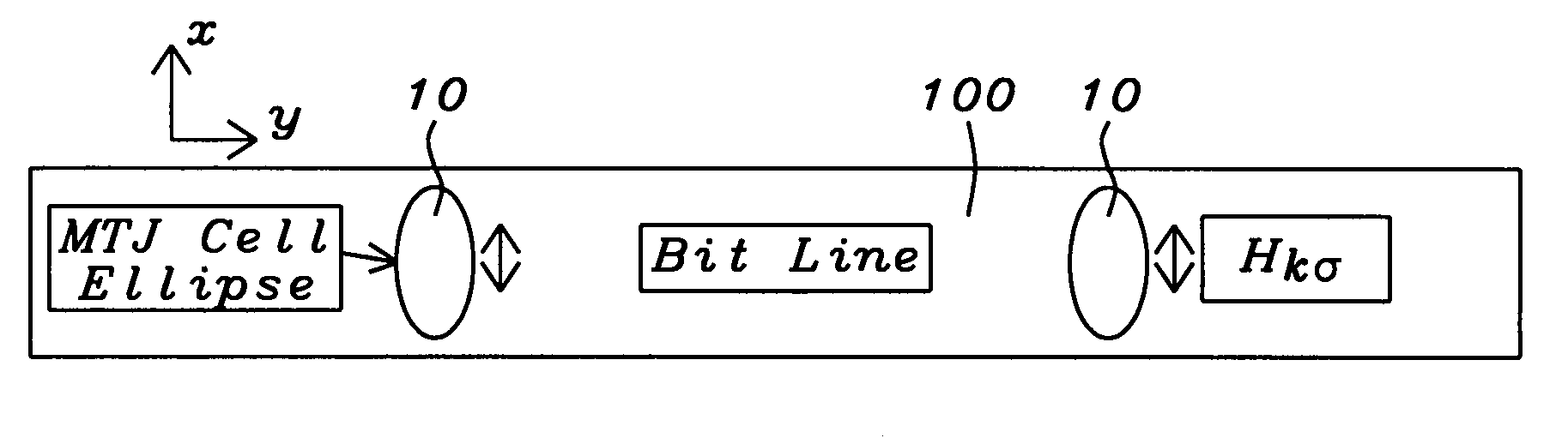
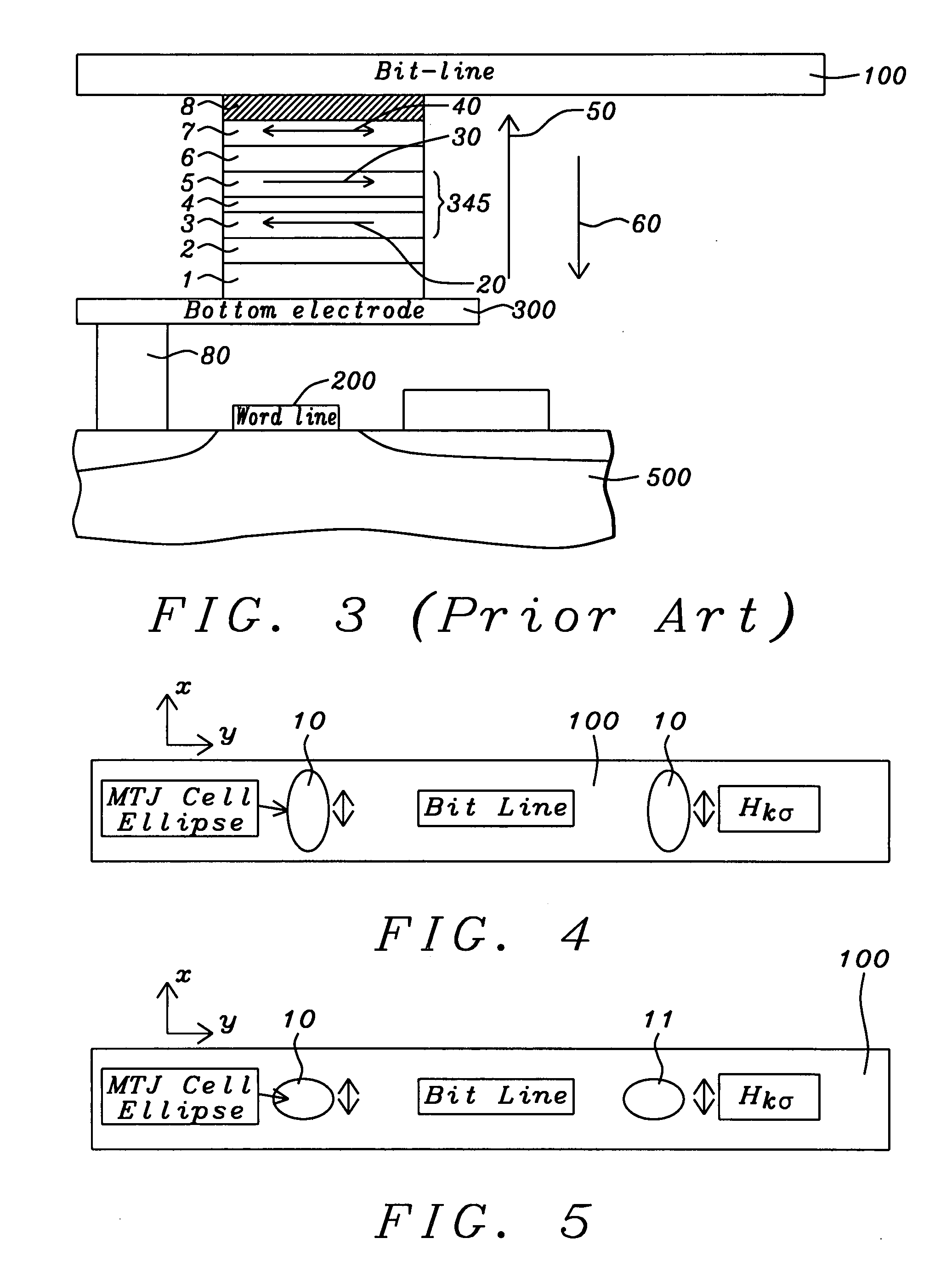
[0037]The preferred embodiment of the present invention is an MRAM cell of the spin-transfer variety, having a CPP-MTJ configuration and including a free layer whose switching field, Hs is a result of a magnetic anisotropy produced by a combination of shape anisotropy and stress-induced magnetostriction. The pinned layer can be a single layer of ferromagnetic material or a synthetic (SyAP) antiferromagnetic layer. As noted above, during operation of the cell, the passage of a current perpendicularly through the free layer produces a torque induced switching of the free layer magnetization due to the interaction of the spins of the conduction electrons with the magnetic moment of the free layer. The torque must be sufficient to switch the magnetization direction, against the countering effect of the switching field. Once the switch is complete, the same switching field provides sufficient magnetic energy to the magnetic moment configuration to stabilize the magnetization against ther...


PUM


Abstract

We describe the manufacturing process for and structure of a CPP MTJ MRAM unit cell that utilizes transfer of spin angular momentum as a mechanism for changing the magnetic moment direction of a free layer. The strength of the switching field, Hs of the cell is controlled by the magnetic anisotropy of the cell which, in turn, is controlled by a combination of the shape anisotropy and the stress and magnetostriction of the cell free layer. The coefficient of magnetostriction of the free layer can be adjusted by methods such as adding Nb or Hf to alloys of Ni, Fe, Co and B or by forming the free layer as a lamination of layers having different values of their coefficients of magnetostriction. Thus, by tuning the coefficient of magnetostriction of the cell free layer it is possible to produce a switching field of sufficient magnitude to render the cell thermally stable while maintaining a desirable switching current.

Description

BACKGROUND OF THE INVENTION[0001]1. Field of the Invention[0002]This invention relates generally to a current perpendicular to plane random access memory (CPP-MRAM) cell formed as a magnetic tunneling junction (MTJ) using a spin transfer effect to change the magnetization of a free layer.[0003]2. Description of the Related Art[0004]The conventional magnetic tunneling junction (MTJ) device is a form of ultra-high magnetoresistive (MR) device in which the relative orientation of the magnetic moments of parallel, vertically separated magnetized layers, controls the flow of spin-polarized electrons tunneling through a very thin dielectric layer (the tunneling barrier layer) formed between those layers. When injected electrons pass through the upper layer they are spin polarized by interaction with the magnetic moment of that layer. The majority of the electrons emerge polarized in the direction of the magnetic moment of the upper layer, the minority being polarized opposite to that dire...

Claims


Application Information

Patent Timeline
IPC IPC(8): H01L43/08H01L43/12
CPCH01L43/12H01L43/08G11C11/1675H10N50/10H10N50/01
Inventor MIN, TAIWANG, PO KANG
Owner TAIWAN SEMICON MFG CO LTD
Why Eureka
Try Eureka