Semiconductor integrated circuit device having control circuit to selectively activate decoupling cells

a technology of integrated circuits and control circuits, applied in pulse manipulation, power consumption reduction, pulse techniques, etc., can solve problems such as power noise increase, and achieve the effect of preventing power noise from increasing

Inactive Publication Date: 2009-04-16
RENESAS ELECTRONICS CORP
View PDF5 Cites 17 Cited by
  • Summary
  • Abstract
  • Description
  • Claims
  • Application Information

AI Technical Summary

Benefits of technology

[0014]As described above, the semiconductor integrated circuit device of the present invention controls the ON/OFF state of each power switch according to the level of the power noise to be varied according to the operation state of the internal circuit. Consequently, the semiconductor integrated circuit device of the present invention can change the resonance frequency of the power line according to the operation state of the internal circuit. This means that the semiconductor in...

Problems solved by technology

If the frequency of this clock signal matches with the resonance freque...

Method used


Image

  • Semiconductor integrated circuit device having control circuit to selectively activate decoupling cells
  • Semiconductor integrated circuit device having control circuit to selectively activate decoupling cells
  • Semiconductor integrated circuit device having control circuit to selectively activate decoupling cells

Examples


first exemplary embodiment

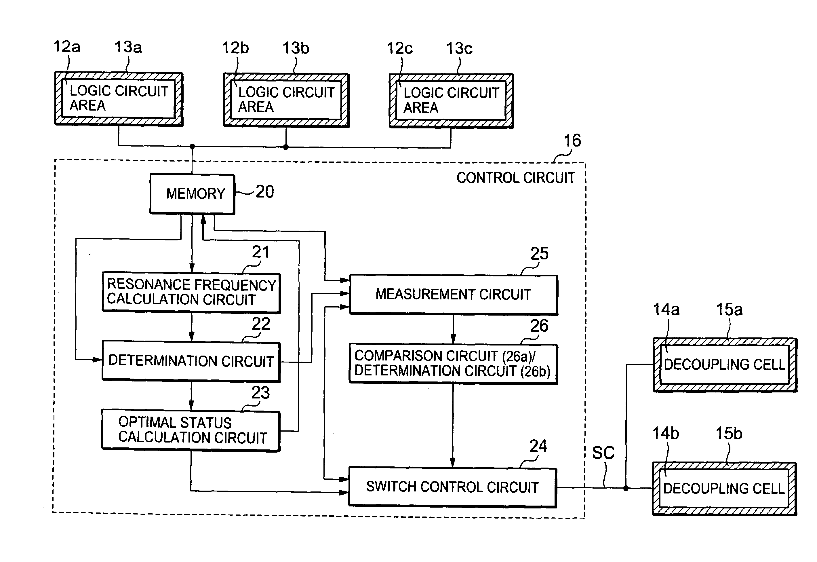
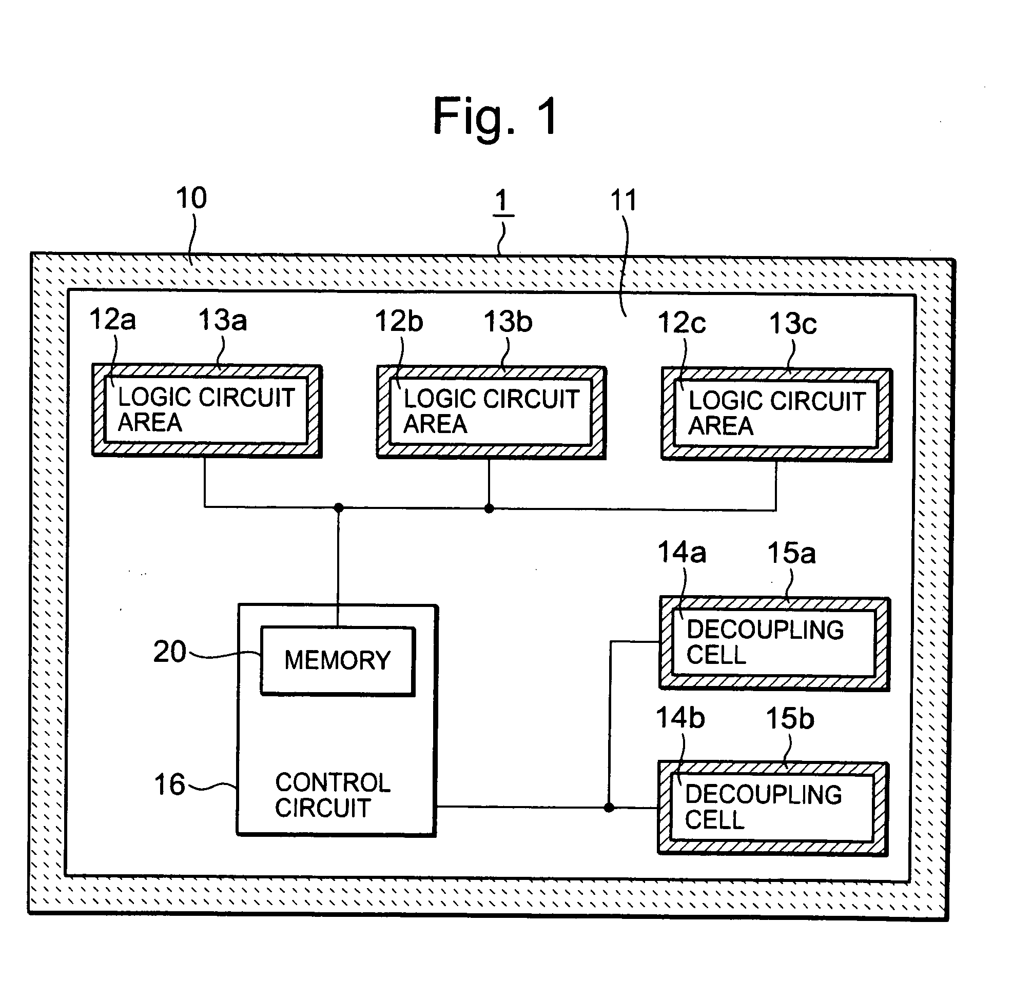
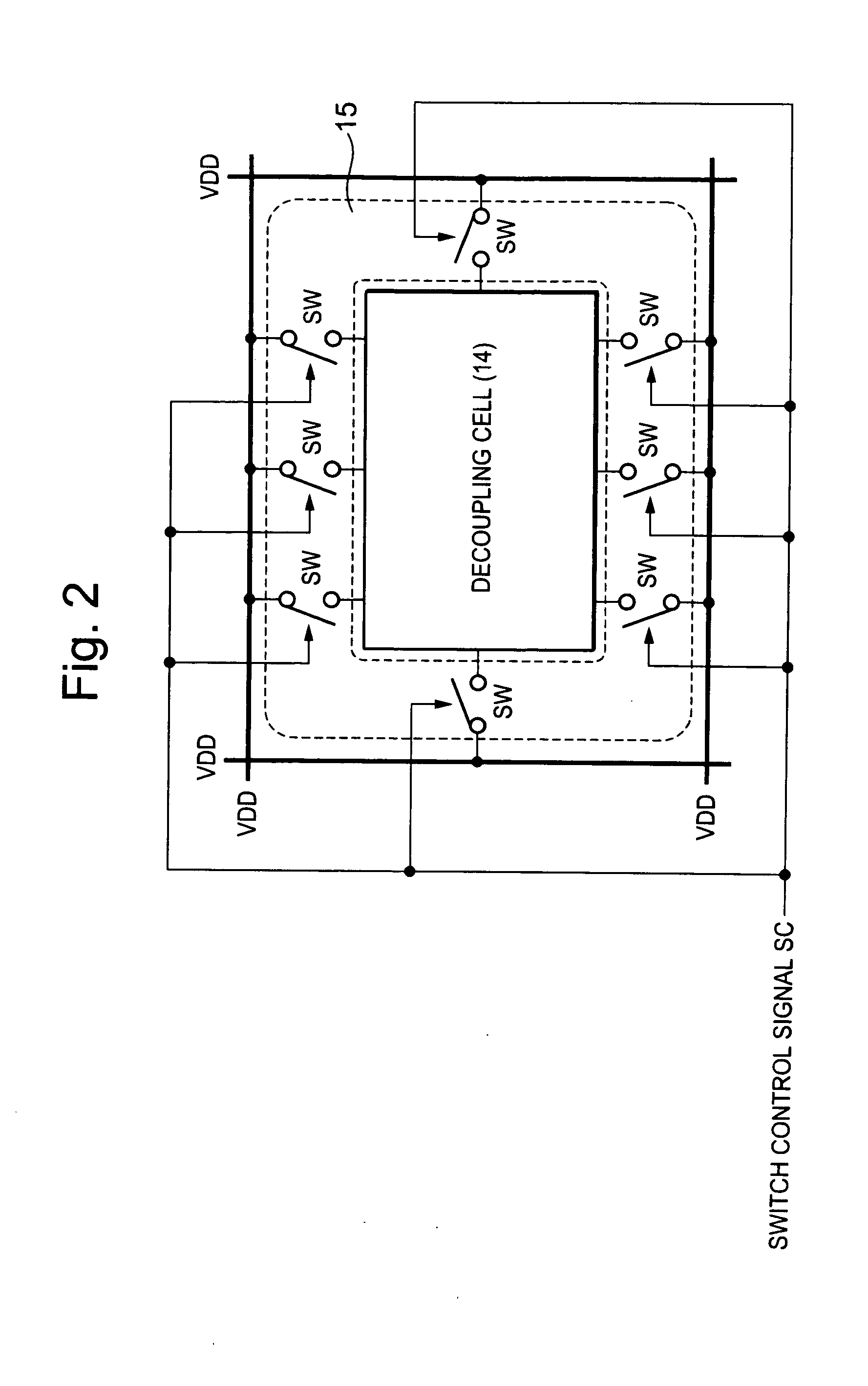
[0031]FIG. 1 shows a block diagram of a semiconductor integrated circuit device 1 in a first exemplary embodiment. The semiconductor integrated circuit device 1 includes an input / output circuit area 10 at the outer periphery of a chip and an internal circuit area 11 inside the area 10. The internal circuit area 11 includes logic circuits 12a to 12c, decoupling cells 14a and 14b, and a control circuit 16 that are combined to form the internal circuit therein.

[0032]Each of the logic circuits 12a to 12c has its corresponding power switch 13a / 13b / 13c disposed around itself. Each power switch supplies a power to its corresponding logic circuit formed in the area. Each logic circuit is driven by a supplied power and according to a clock signal inputted from external. The power switches 13a to 13c, when turned on respectively, supply a power to their corresponding logic circuits. When the power switches 13a to 13c are turned OFF, they stop the power supply to the logic circuits. A power co...

second exemplary embodiment

[0054]FIG. 8 shows a block diagram of a semiconductor integrated circuit device in a second exemplary embodiment. In this second exemplary embodiment, the same reference numerals will be used for the same components as those in the first exemplary embodiment, avoiding redundant description. As shown in FIG. 8, the semiconductor integrated circuit device 2 includes a control circuit 16a. The control circuit 16a inputs package information and clock signal frequency information from external. FIG. 9 shows a block diagram of the control circuit 16a.

[0055]As shown in FIG. 9, the control circuit 16a excludes the memory 20, the measurement circuit 25, and the comparison circuit / decision circuit 26 from the control circuit 16. In the control circuit 16a, the resonance frequency calculation circuit 21 inputs operation mode signals directly from the logic circuits 12a to 12c. The resonance frequency calculation circuit 21 also inputs package information directly from external and the decisio...

third exemplary embodiment

[0058]FIG. 11 shows a block diagram of a semiconductor integrated circuit device 3 in a third exemplary embodiment. The semiconductor integrated circuit device 3 includes an internal circuit forming area divided into a plurality of areas (AREA1 to AREA4 shown in FIG. 11). Each of the areas includes a plurality of decoupling cells 14a to 14f and a control circuit 16. Although not shown inFIG. 11, it is premised that a plurality of logic circuit forming areas are formed in the semiconductor integrated circuit device 3. In this third exemplary embodiment, the same reference numerals will be used for the same components as those in the first embodiment, avoiding redundant description.

[0059]This third exemplary embodiment includes a control circuit 16b, which is a variation of the control circuit 16. FIG. 12 shows a block diagram of the control circuit 16b. As shown in FIG. 12, the control circuit 16b deletes the resonance frequency calculation circuit 21, the decision circuit 22, and th...


PUM


Abstract

The semiconductor integrated circuit device includes a plurality of decoupling cells that suppress power noise respectively, a plurality of power switches that connect the decoupling cells to a power line respectively, and a control circuit that controls the number of power switches selected from among the plurality of power switches and to be turned on according to power noise to be changed according to the operation state of each of internal circuits driven by a power supplied from the power line.

Description

BACKGROUND OF THE INVENTION[0001]1. Field of the Invention[0002]The present invention relates to a semiconductor integrated circuit device, particularly to a semiconductor integrated circuit device that includes a decoupling cell that suppresses power noise.[0003]2. Description of Related Art[0004]In recent years, the supply voltage of semiconductor integrated circuit devices has become lower and the power noise has affected more significantly operations of the circuits of those devices. This is why such semiconductor integrated circuit devices have come to include a decoupling capacitor provided between a power line and a ground line to stabilize the supply voltage respectively. The patent document 1 (hereunder, to be referred to as the conventional example 1) discloses an example of such a decoupling capacitor that can be built in such semiconductor integrated circuit devices.[0005]A semiconductor integrated circuit device, when including a plurality of circuit blocks therein, cha...

Claims


Application Information

Patent Timeline
IPC IPC(8): H03K5/00
CPCH03K19/0008
Inventor NAKASHIMA, HIDENARI
Owner RENESAS ELECTRONICS CORP
Why Eureka
Try Eureka