
Semiconductor laser apparatus and method of manufacturing the same

a laser apparatus and semiconductor technology, applied in the direction of lasers, semiconductor laser arrangements, semiconductor lasers, etc., can solve the problems of difficult downsizing of dvd drives, increasing the number of components, and cost, and achieves convenient processing, improved processability, and easy cleavability

Inactive Publication Date: 2009-04-16
SANYO ELECTRIC CO LTD
View PDF17 Cites 4 Cited by
  • Summary
  • Abstract
  • Description
  • Claims
  • Application Information

AI Technical Summary

Benefits of technology

[0018]Therefore, a common optical system can be employed for the light beams emitted from the emission points of the first, second and third semiconductor laser devices respectively. Consequently, the first, second and third semiconductor laser devices are improved in light extraction efficiency when the light beams emitted from the emission points are condensed through a lens.
[0168]Further, the thinly processed second growth substrate is easily cleavable. Thus, the stacked substrate is so easily cleavable that cavity facets of the first and second semiconductor laser devices can be easily formed. Further, flat cavity facets can be easily obtained.

Problems solved by technology

According to this method, however, the number of components is so increased that it is difficult to downsize the DVD drive, simplify the structure thereof and reduce the cost therefor.
However, while the infrared semiconductor laser device and the red semiconductor laser device formed on GaAs substrates can be integrated into one chip, it is extremely difficult to integrate a blue-violet semiconductor laser device not formed on a GaAs substrate with the infrared and red semiconductor laser devices into one chip.
In the aforementioned light-emitting device, however, the infrared and blue-violet semiconductor laser devices share a common electrode in structure, and hence it is difficult to individually apply arbitrary voltages to the infrared semiconductor laser device, the red semiconductor laser device and the blue-violet semiconductor laser device respectively by a driving circuit.
Therefore, the structure of the driving circuit has low flexibility, leading to a complicated structure.
Thus, the driving system for the infrared semiconductor laser device and the blue-violet semiconductor laser device is inevitably limited.

Method used


Image

  • Semiconductor laser apparatus and method of manufacturing the same
  • Semiconductor laser apparatus and method of manufacturing the same
  • Semiconductor laser apparatus and method of manufacturing the same

Examples


first embodiment

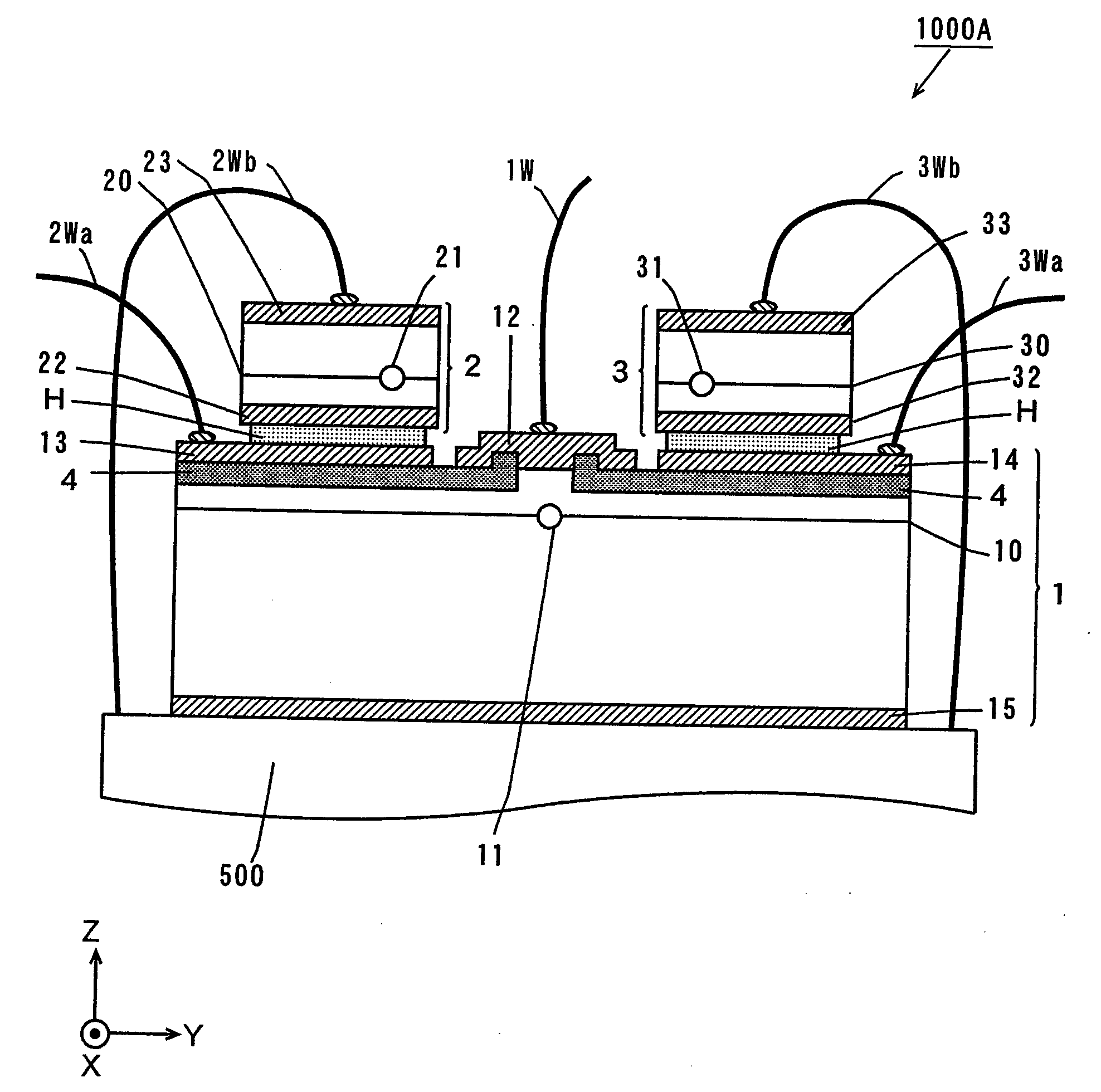
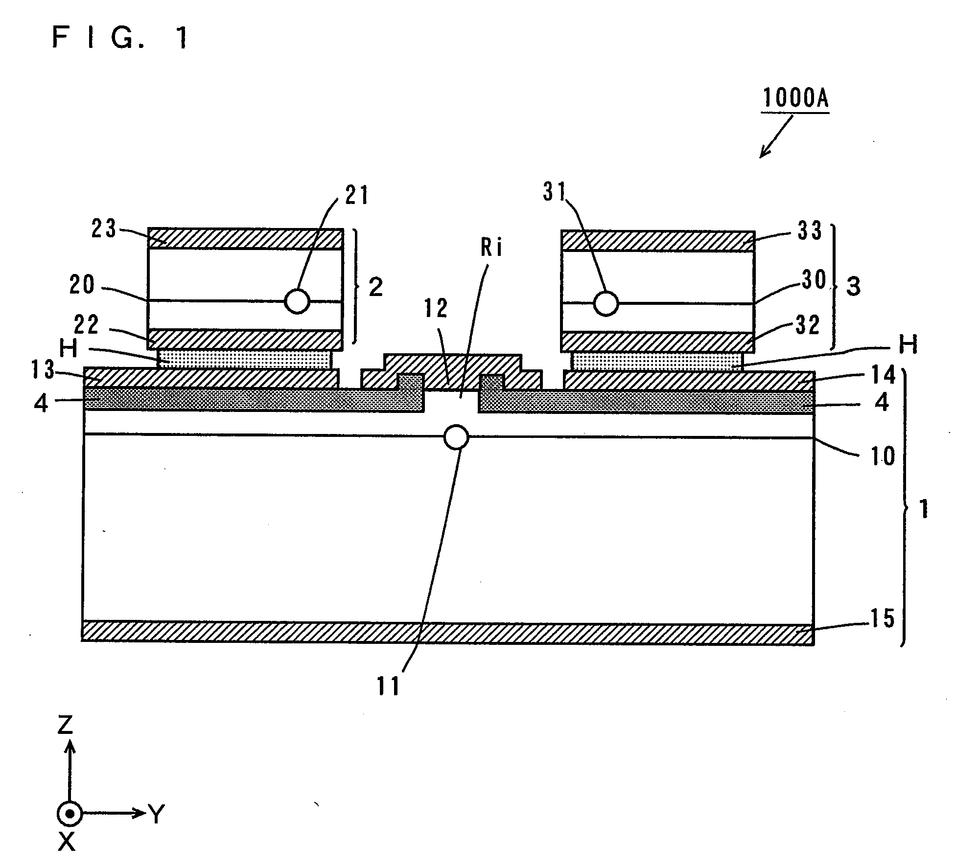
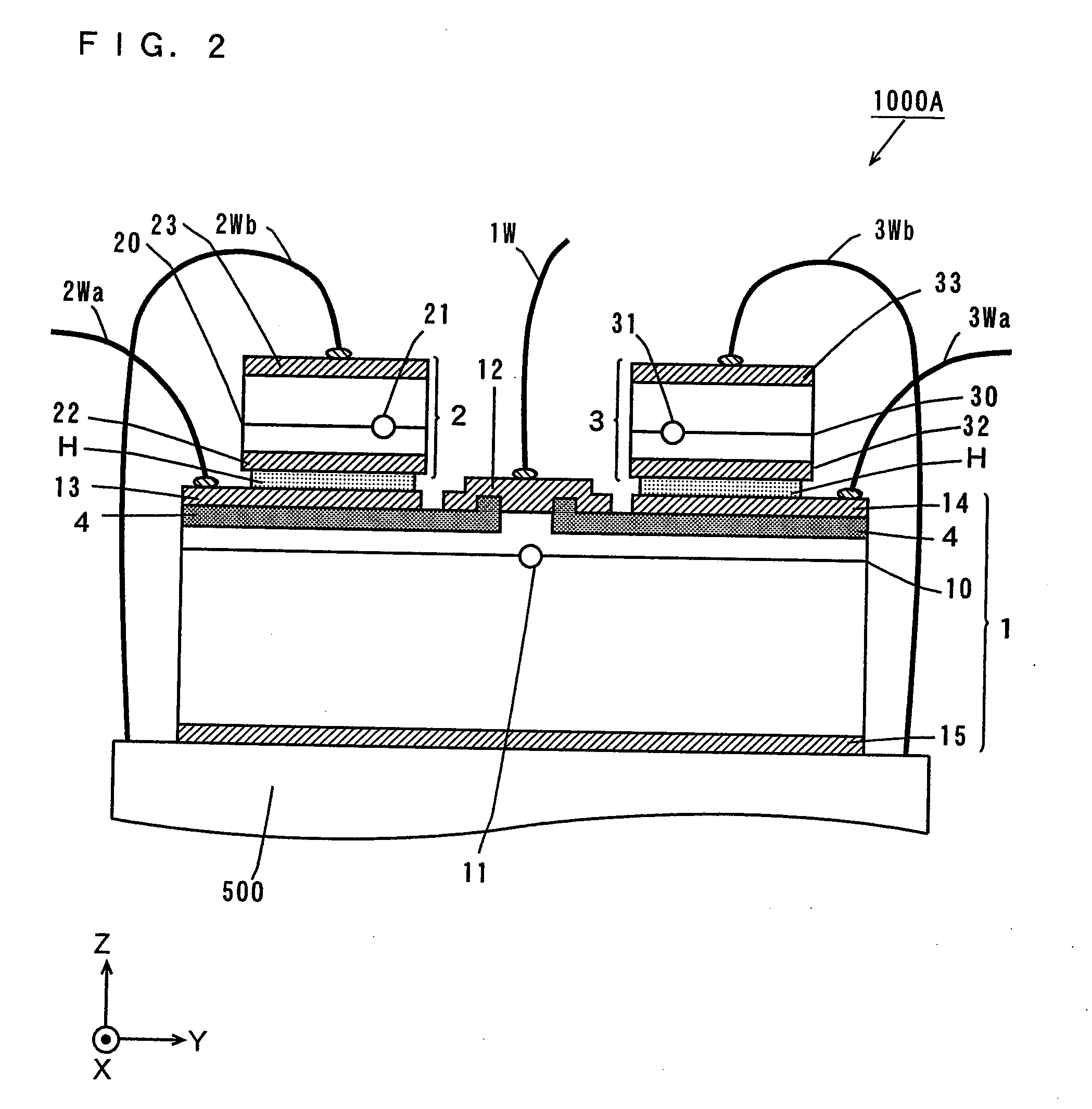
[0192]FIG. 1 is a schematic sectional view showing an exemplary semiconductor laser apparatus 1000A according to a first embodiment of the present invention.

[0193]The semiconductor laser apparatus 1000A according to the first embodiment comprises a semiconductor laser device (hereinafter referred to as a blue-violet semiconductor laser device) 1 emitting a laser beam having a wavelength of about 400 nm, a semiconductor laser device (hereinafter referred to as a red semiconductor laser device) 2 emitting a laser beam having a wavelength of about 650 nm and a semiconductor laser device (hereinafter referred to as an infrared semiconductor laser device) 3 emitting a laser beam having a wavelength of about 780 nm.

[0194]According to the first embodiment, the blue-violet semiconductor laser device 1 is prepared by forming a semiconductor layer on a GaN substrate. The red semiconductor laser device 2 and the infrared semiconductor laser device 3 are prepared by forming semiconductor layers...

second embodiment

[0469]FIGS. 32(a) and 32(b) are schematic diagrams showing an exemplary semiconductor laser apparatus 1000B according to a second embodiment of the present invention. Also in the following description, directions X, Y and Z are defined similarly to those in FIG. 1.

[0470]The semiconductor laser apparatus 1000B according to the second embodiment is different in structure from the semiconductor laser apparatus 1000A according to the first embodiment in the following point:

[0471]FIGS. 32(a) and 32(b) are a schematic sectional view and a plan view of the semiconductor laser apparatus 1000B respectively.

[0472]As shown in FIG. 32(a) and 32(b), a p-side pad electrode 12 of a blue-violet semiconductor laser device 1 extends in a direction (direction Y) on an insulating film 4 to project on the entire surface of an insulating film 4 on the side of the infrared semiconductor laser device 3. Another insulating film 4b is formed on the p-side pad electrode 12. The insulating film 4b is partially...

third embodiment

[0477]FIG. 33 is a schematic sectional view showing an exemplary semiconductor laser apparatus 1000C according to a third embodiment of the present invention. Also in the following description, directions X, Y and Z are defined similarly to those in FIG. 1.

[0478]The semiconductor laser apparatus 1000C according to the third embodiment is different in structure from the semiconductor laser apparatus 1000B according to the second embodiment in the following point:

[0479]As shown in FIG. 33, red and infrared semiconductor laser devices 2 and 3 bonded onto a blue-violet semiconductor laser device 1 are integrally formed in the third embodiment. The combination of the integrally formed red and infrared semiconductor laser devices 2 and 3 is hereinafter referred to as a monolithic red / infrared semiconductor laser device 23X.

[0480]In preparation of this monolithic red / infrared semiconductor laser device 23X, neither etching stopper layer 51 nor n-GaAs contact layer 5 may be formed on an n-G...


PUM


Abstract

Second and third p-side pad electrodes are formed on an insulating film of a blue-violet semiconductor laser device on both sides of a first p-side pad electrode. The second p-side pad electrode and the third p-side pad electrode are formed separately from each other. Solder films are formed on the upper surfaces of the second and third p-side pad electrodes respectively. A fourth p-side pad electrode of a red semiconductor laser device is bonded onto the second p-side pad electrode with the corresponding solder film sandwiched therebetween. A fifth p-side pad electrode of an infrared semiconductor laser device is bonded onto the third p-side pad electrode with the corresponding solder film sandwiched therebetween. The second and third p-side pad electrodes are formed separately from each other, so that the fourth and fifth p-side pad electrodes are electrically isolated from each other.

Description

BACKGROUND OF THE INVENTION[0001]1. Field of the Invention[0002]The present invention relates to a semiconductor laser apparatus capable of emitting a plurality of light beams having different wavelengths and a method of manufacturing the same.[0003]2. Description of the Background Art[0004]A semiconductor laser device (infrared semiconductor laser device) emitting infrared light having a wavelength of about 780 nm has generally been applied to a CD (compact disk) / CD-R (compact disk-recordable) drive as a light source. Further, a semiconductor laser device (red semiconductor laser device) emitting red light having a wavelength of about 650 nm has been applied to a DVD (digital versatile disk) drive as a light source.[0005]On the other hand, a DVD capable of recording and playback with blue-violet light having a wavelength of about 405 nm has recently been developed. In order to record and play this DVD, a DVD drive employing a semiconductor laser device (blue-violet semiconductor la...

Claims


Application Information

Patent Timeline
Patent Type & Authority Applications(United States)
IPC IPC(8): H01S5/00H01L21/00H01S5/026H01S5/22H01S5/40
CPCH01S5/4087H01S5/4025
Inventor BESSHO, YASUYUKIHATA, MASAYUKIINOUE, DAIJIRO
Owner SANYO ELECTRIC CO LTD
Learn More