Substrate treating apparatus and method of manufacturing the same

a technology of substrate and treating apparatus, which is applied in the direction of manufacturing tools, cleaning using liquids, transportation and packaging, etc., can solve the problems of high accuracy and complicated process, and the requirement of large-diameter wafers, so as to facilitate assembling/disassembling and maintenance/repair

Active Publication Date: 2009-04-23
SEMES CO LTD
View PDF16 Cites 14 Cited by
  • Summary
  • Abstract
  • Description
  • Claims
  • Application Information

AI Technical Summary

Problems solved by technology

In recent, with the tendency toward miniaturization and high integration of semiconductor devices, a highly accurate and complicated process and a large-diameter wafer are required.

Method used


Image

  • Substrate treating apparatus and method of manufacturing the same
  • Substrate treating apparatus and method of manufacturing the same
  • Substrate treating apparatus and method of manufacturing the same

Examples


embodiment

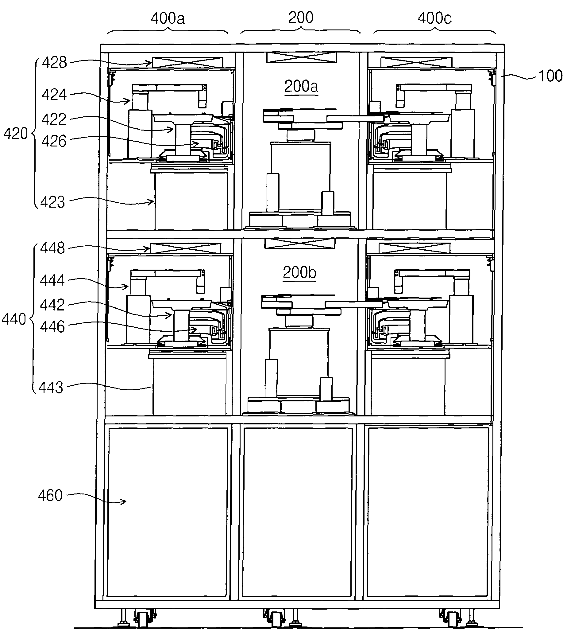
[0034]Though a substrate cleaning apparatus is exemplary described in this embodiment, the present invention is not limited thereto. The present invention may be applied to a multi-chamber type semiconductor manufacturing apparatus performing different substrate treating processes except a cleaning process.

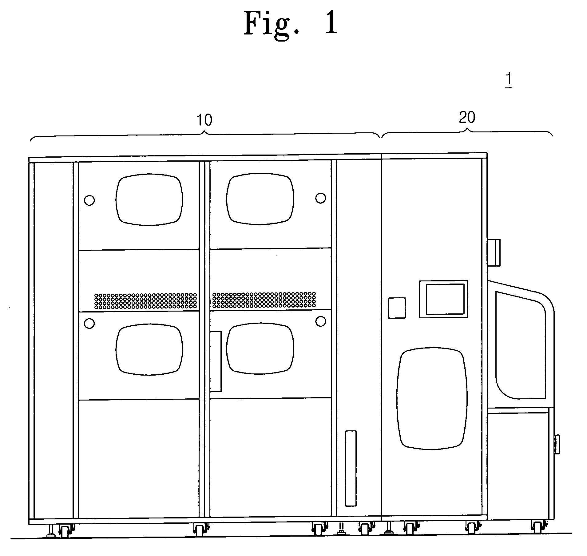
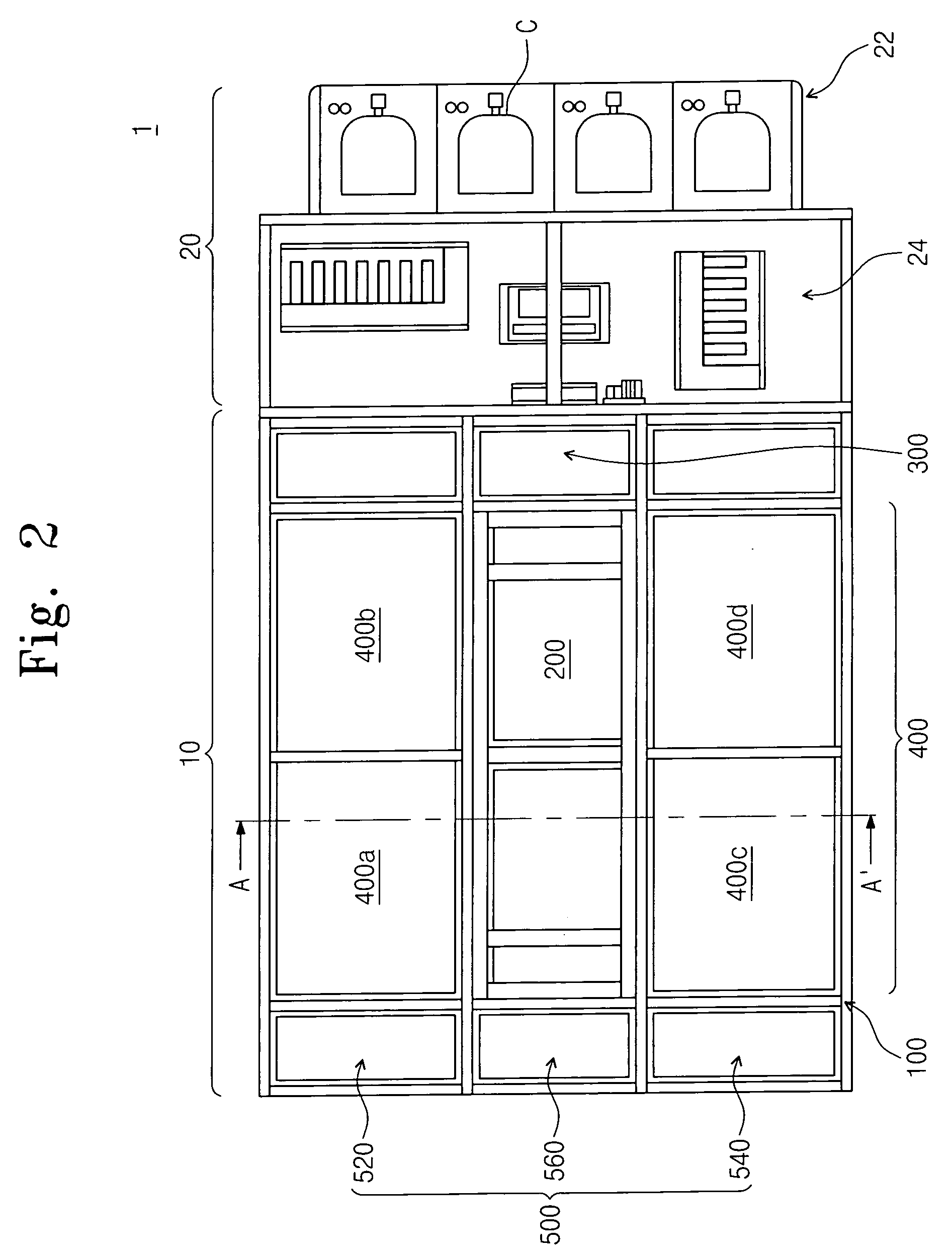
[0035]FIG. 1 is a front view of a substrate treating apparatus according to the present invention, and FIG. 2 is a top view of a substrate treating apparatus according to the present invention.

[0036]Referring to FIGS. 1 and 2, a substrate treating apparatus 1 for cleaning a substrate according to the present invention includes a process equipment 10 and an equipment front end module 20. In the process equipment 10, a cleaning process is performed using a single wafer processing method. The equipment front end module 20 is disposed at a front side of the process equipment 10. The equipment front end module 20 transfers the substrate between a container C receiving the substrate and...


PUM

PropertyMeasurementUnit
diameteraaaaaaaaaa
air currentaaaaaaaaaa
chemicalaaaaaaaaaa

Abstract

Provided are a substrate treating apparatus and a method of manufacturing the substrate treating apparatus. Processing units of a process equipment are modularized, and the modularized processing units are detachably disposed in a main frame. According to this characteristic, work time and work effort required for manufacturing the process equipment can be reduced. In addition, maintenance / repair of each of the processing units can be further easily performed.

Description

CROSS-REFERENCE TO RELATED APPLICATION[0001]This U.S. non-provisionial patent application claims priority under 35 U.S.C. §119 of Korean Patent Application No. 10-2007-0106548, filed on Oct. 23, 2007, the entire contents of which are hereby incorporated by reference.BACKGROUND OF THE INVENTION[0002]The present invention disclosed herein relates to a substrate treating apparatus and a method of manufacturing the same, and more particularly, a substrate treating apparatus of a module assembly type and a method of manufacturing the same.[0003]In a manufacture of a semiconductor device, various materials are deposited in thin film forms onto a wafer, and then patterned to form the semiconductor device. For this, various different processes such as a deposition process, an etching process, a cleaning process, and a drying process are required. During each of the processes, the wafer is loaded / treated into / in a process chamber having an optimum condition for the corresponding process.[000...

Claims


Application Information

Patent Timeline
Patent Type & Authority Applications(United States)
IPC IPC(8): B05C13/00H01L21/67
CPCH01L21/67161H01L21/67184H01L21/6719Y10T29/49826H01L21/67207Y10S134/902H01L21/67196H01L21/02
Inventor JANG, SUNG-HOKANG, BYUNG-MAN
Owner SEMES CO LTD
Why Eureka
Try Eureka