Dual-View Display Panel Structure and Method for Producing the Same
a display panel and dual-view technology, applied in the manufacture of electrode systems, electric discharge tubes/lamps, instruments, etc., can solve the problems of increasing production yield, achieve the effect of reducing the number of glass layers required, improving the light transmission of the display panel, and widening the viewing angle rang
- Summary
- Abstract
- Description
- Claims
- Application Information
AI Technical Summary
Benefits of technology
Problems solved by technology
Method used
Image
Examples
first embodiment
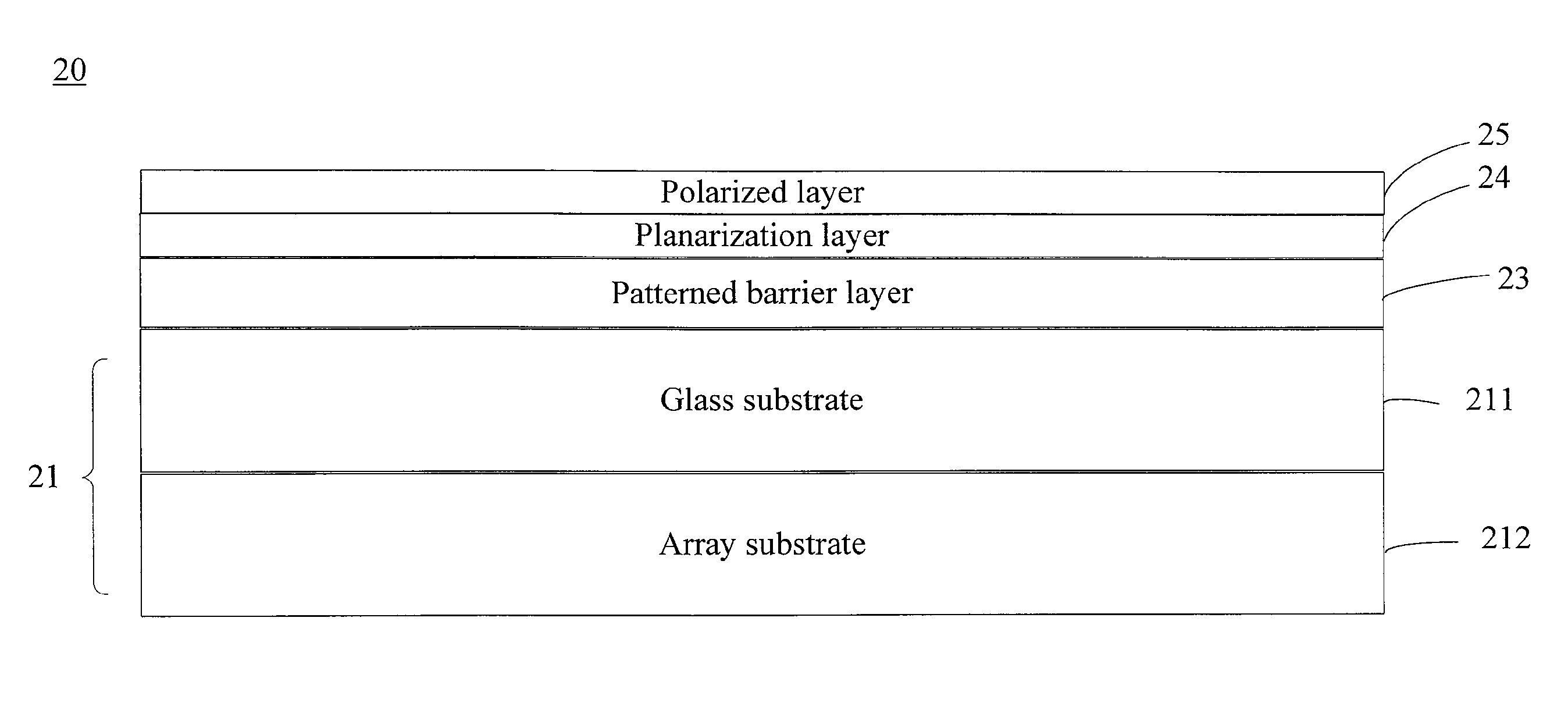
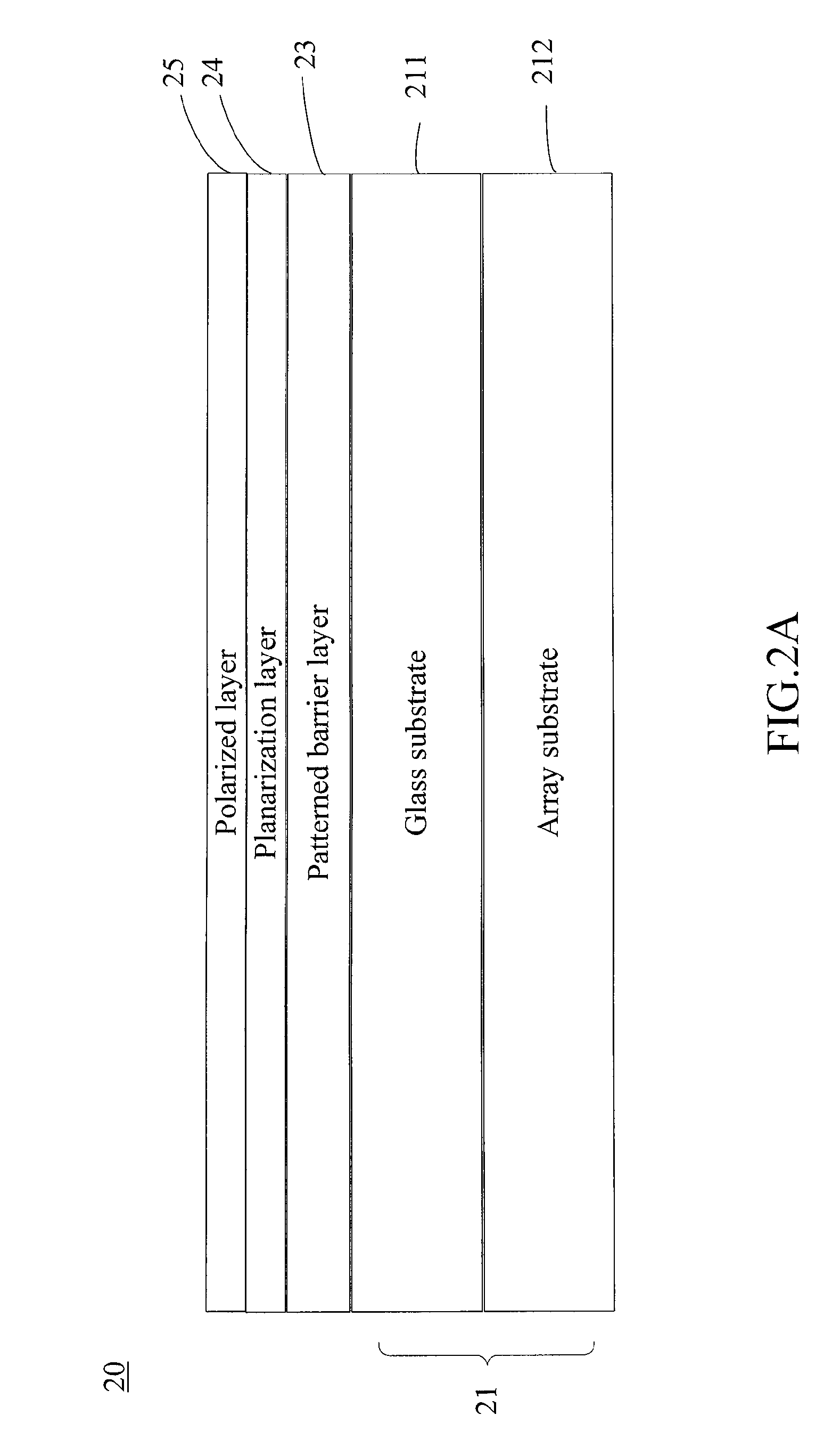
[0031]FIG. 2A depicts this invention, which is a dual-view display panel structure 20. The dual-view display panel structure 20 comprises a display panel 21, a patterned barrier layer 23, a planarization layer 24 and a polarized layer 25. The display panel 21 comprises at least one glass substrate 211, for example, a color filter substrate. In addition, the display panel 21 further comprises an array substrate 212, and may also comprise other conventional display elements, such as a pixel layer (not shown) formed on the glass substrate 211 and an liquid crystal (LC) layer (not shown) formed between the array substrate 212 and the glass substrate 211. The glass substrate 211 is adapted to form the patterned barrier layer 23 on a surface thereof. The patterned barrier layer 23 is adapted to yield a dual-view effect. The planarization layer 24 is an organic material layer formed on the patterned barrier layer 23 to provide a relatively planar surface so that the possibility of gap form...
second embodiment
[0038]FIG. 3A depicts this invention, which is a dual-view display panel structure 30. The dual-view display panel structure 30 comprises a first substrate 31, a patterned barrier layer 32, a transparent material layer 33, a planarization layer 34, a pixel layer 35 and a second substrate 36.
[0039]The first substrate 31 is a glass substrate to be a color filter substrate. The patterned barrier layer 32 is formed on the first substrate 31 for yielding a dual-view effect. The transparent material layer 33, which is made of a transparent macromolecular material, is in turn formed on the patterned barrier layer 32 to combine with the patterned barrier layer 32 to yield a dual-view effect. The planarization layer 34, which is made of an organic material, is formed on the transparent material layer 33, and is adapted to control the uniformity in the thickness of the transparent material layer 33. The pixel layer 35 is formed on the planarization layer 34, and is for example, a color filter...
third embodiment
[0044]FIG. 4A depicts this invention, which is a dual-view display panel structure 40. The dual-view display panel structure 40 comprises a transparent substrate 41, a patterned barrier layer 42, a transparent material layer 43, and a display panel 44. The patterned barrier layer 42 is formed on the transparent substrate 41 for yielding a dual-view displaying effect. In application, the display panel 44 may comprise a first substrate 441, a pixel layer 442 formed on the first substrate 441, an LC layer 443 and a second substrate 444, in which the LC layer 443 is disposed between the pixel layer 442 and the second substrate 444. The transparent material layer 43 is made of a liquid transparent material and is formed in a gap between the patterned barrier layer 42 and the first substrate 441 of the display panel 44.
[0045]In this embodiment, the transparent substrate 41 with the patterned barrier layer 42 formed thereon is attached to the first substrate 441 of the display panel 44 to ...
PUM
 Abstract
Description
Claims
Application Information


