Three-dimensional memory module architectures

a memory module and three-dimensional technology, applied in the field of stacking three-dimensional memory modules, can solve the problems of increasing the cost of memory modules, and increasing the performance of main memory systems without a commensurate increase in energy consumption or cos

Active Publication Date: 2009-04-23
HEWLETT-PACKARD ENTERPRISE DEV LP
View PDF27 Cites 154 Cited by
  • Summary
  • Abstract
  • Description
  • Claims
  • Application Information

AI Technical Summary

Problems solved by technology

An intrinsic problem shared by all computer systems is the need for increased main memory system performance without a commensurate increase in energy consumption or cost.
Electrical communication architectures struggle to balance the dichotomy for increased performance required of electronic systems while addressing lower power consumption, smaller form factor, and lower electromagnetic emissions.
However, typical electronic solutions to these problems often increase the cost of the memory modules either because of increased pin count and / or die area, or increased power consumption, a major cause of which is the need to communicate over long wires.
However, typical electronic solutions to these problems often increase the cost of the memory modules either because of increased pin count and / or die area, or increased power consumption.
As mentioned above, a major cause of the increased power consumption is the need to communicate over long wires.
Increasing the front side bus speed also causes a linear increase in interface power consumption.
An additional interconnect issue with increasing the number of DIMM ranks at increased front side bus speeds is that both signal timing and noise are problems in the multi-drop wires that connect multiple DIMMs.
This so called “stub electronics” problem has led to memory buses being replaced by point to point memory channels requiring additional external buffers to interface to the DRAMs.

Method used


Image

  • Three-dimensional memory module architectures
  • Three-dimensional memory module architectures
  • Three-dimensional memory module architectures

Examples


Embodiment Construction

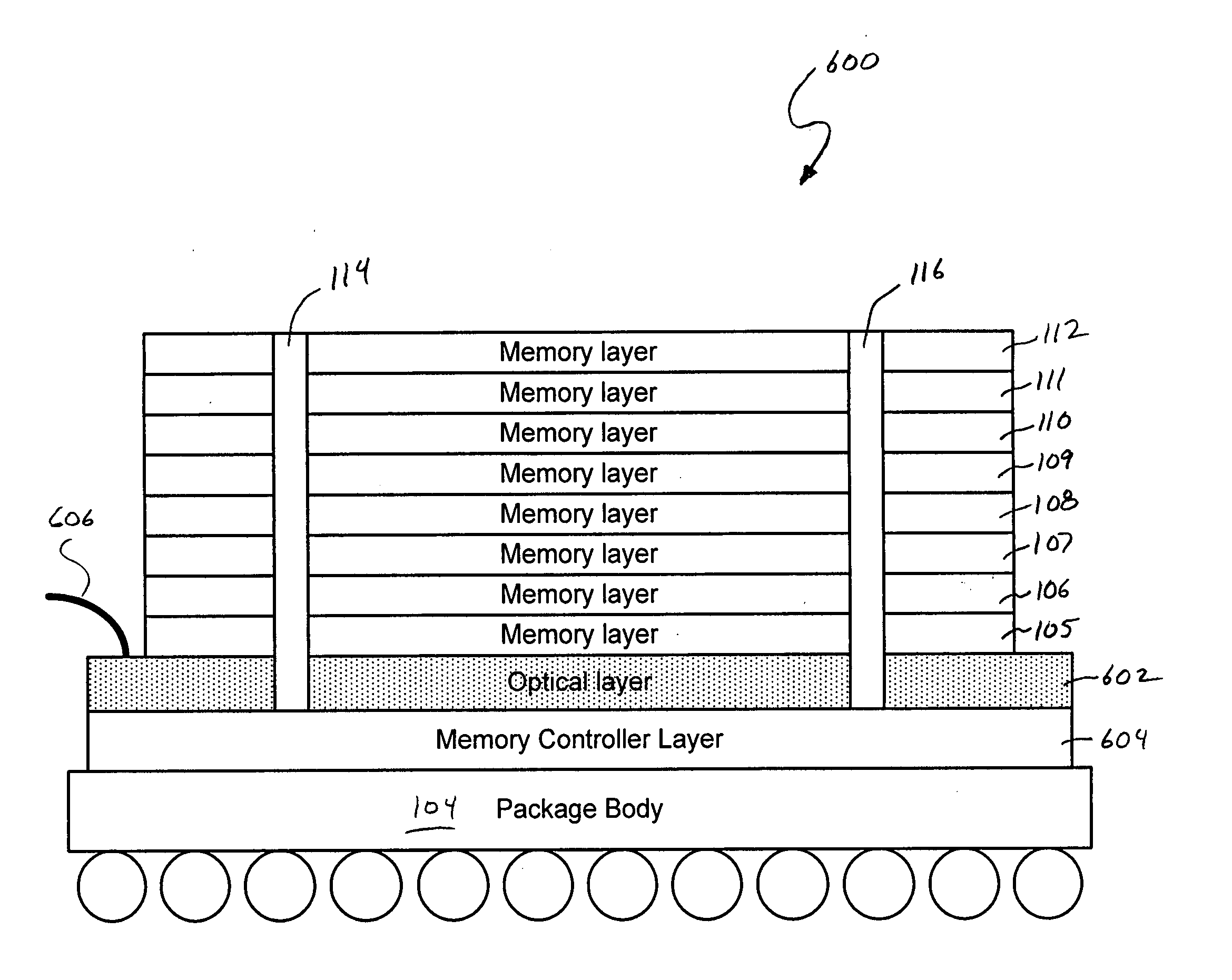
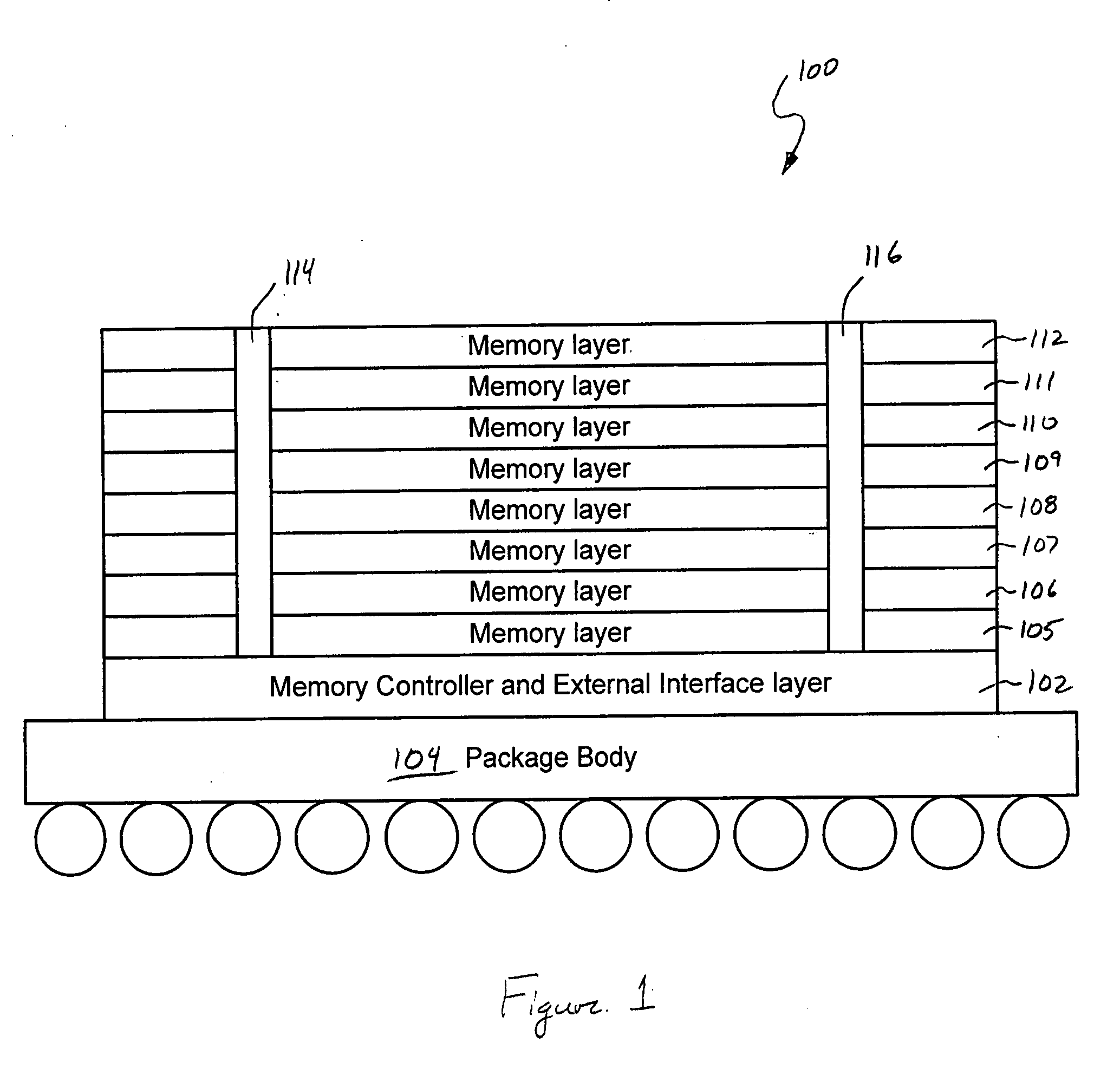
[0024]Embodiments of the present invention are directed to stacked, three-dimensional memory modules including multiple internal data buses for reducing internal interconnect delays. The multiple internal data buses are implemented using through silicon vias allowing the memory modules to be organized as many small, high bandwidth sub-blocks leading to reduced access time and reduced power consumption.

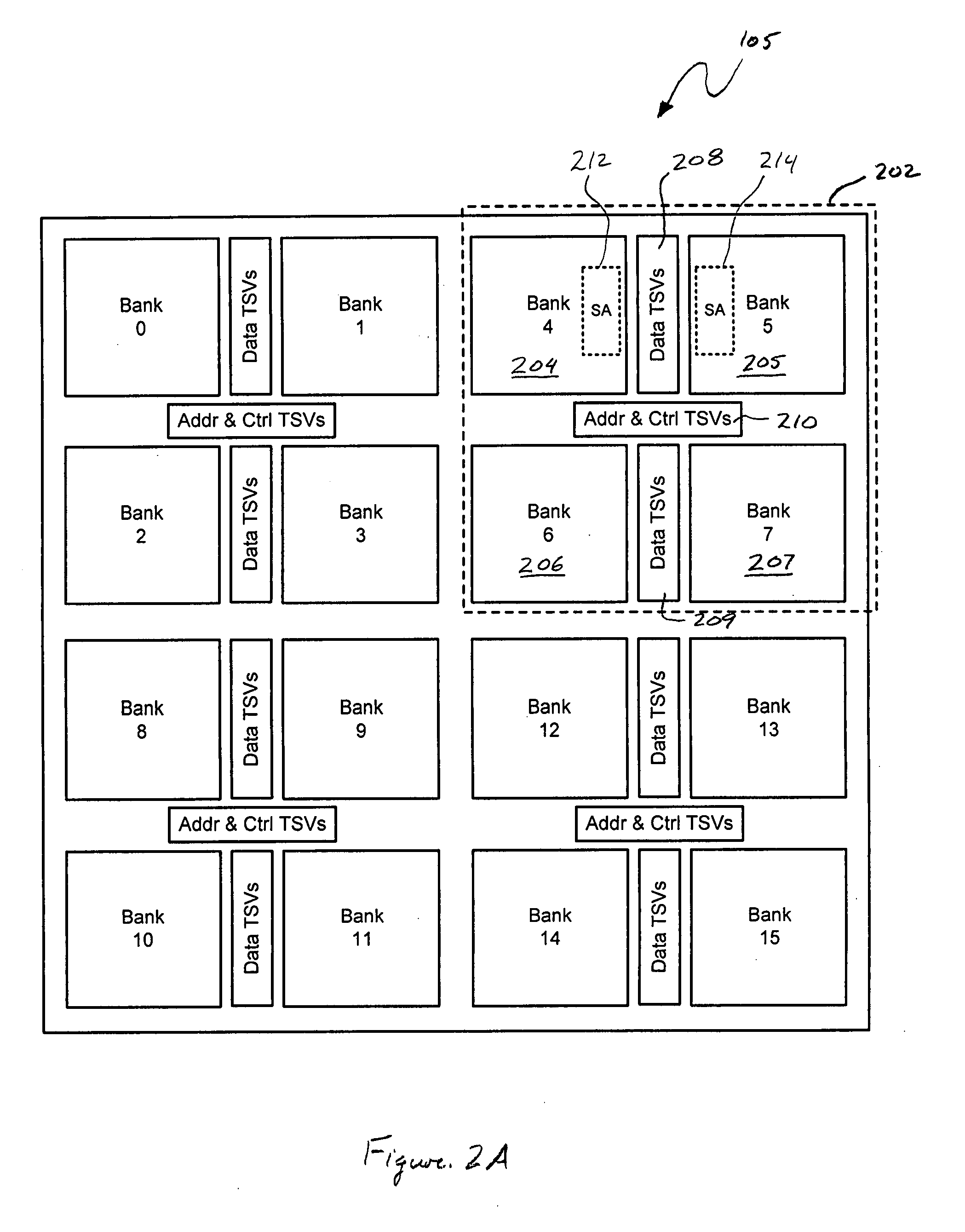
[0025]FIG. 1 shows a cross-sectional view of a three-dimensional, electronic memory module (“memory module”) 100 in accordance with embodiments of the present invention. In the illustrated example, the memory module 100 includes a memory-controller layer 102 disposed on the top surface of a package body 104 and a stack of eight individual memory layers 105-112 disposed on the top surface of the memory-controller layer 102. The memory layers 105-112 can be volatile memory layers, such as DRAM, non-volatile memory layers, or a combination of volatile and non-volatile memory layers. The m...


PUM


Abstract

Various embodiments of the present invention are directed to stacked memory modules. In one embodiment of the present invention, a memory module comprises at least one memory-controller layer stacked with at least one memory layer. Fine pitched through vias (e.g., through silicon vias) extend approximately perpendicular to a surface of the at least one memory controller through the stack providing electronic communication between the at least one memory controller and the at least one memory layers. Additionally, the memory-controller layer includes at least one external interface configured to transmit data to and from the memory module. Furthermore, the memory module can include an optical layer. The optical layer can be included in the stack and has a bus waveguide to transmit data to and from the at least one memory controller. The external interface can be an optical external interface which interfaces with the optical layer.

Description

CROSS REFERENCE TO RELATED APPLICATIONS[0001]This patent application may contain subject matter related to the following patent applications, all of which are hereby incorporated by reference: (1) U.S. patent application entitled “PHOTONIC INTERCONNECTS FOR COMPUTER SYSTEM DEVICES,” having inventors Raymond G. Beausoleil, Marco Fiorentino, Norman Paul Jouppi, Qianfan Xu, Robert Samuel Schreiber, and Nathan Lorenzo Binkert having attorney docket no. 200704210-1; and (2) U.S. patent application entitled “THREE-DIMENSIONAL DIE STACKS WITH INTER-DEVICE AND INTRA-DEVICE OPTICAL INTERCONNECT” having inventors Nathan Lorenzo Binkert; Norman Paul Jouppi; Alan Lynn Davis, and Raymond G. Beausoleil having attorney docket no. 200701582-1.TECHNICAL FIELD[0002]Embodiments of the present invention are directed to stacked three-dimensional memory modules.BACKGROUND[0003]An intrinsic problem shared by all computer systems is the need for increased main memory system performance without a commensura...

Claims


Application Information

Patent Timeline
Patent Type & Authority Applications(United States)
IPC IPC(8): G11C5/06G11C13/04
CPCG11C5/02G11C5/025G11C5/04G11C13/04G11C2213/71H01L25/0657H01L2225/06541H01L2924/0002H01L2924/15311H01L2225/06534H01L25/18H01L2225/06565H01L2924/00G11C2211/4016
Inventor MCLAREN, MORAYAHN, JUNG HODAVIS, ALAN LYNNBINKERT, NATHAN LORENZOJOUPPI, NORMAN PAUL
Owner HEWLETT-PACKARD ENTERPRISE DEV LP
Why Eureka
Try Eureka