Global shutter pixel circuit with transistor sharing for CMOS image sensors

a technology of image sensor and transistor, applied in the field of global shutter pixel circuit, can solve the problems of increasing the number of transistors per pixel, the inability to perform global shutter operation, and the inability to achieve global shutter operation, so as to reduce the average transistor count per pixel

Inactive Publication Date: 2009-04-30
ALTASENS
View PDF2 Cites 87 Cited by
  • Summary
  • Abstract
  • Description
  • Claims
  • Application Information

AI Technical Summary

Benefits of technology

[0010]The present invention is a pixel circuit having a global shutter and includes pixel sharing to reduce the average transistor count per pixel. In one embodiment, a circuit includes an imaging pixel with pinned photodiode that simultaneously forms a synchronous image in a block comprising from 2 through N pixels. The photodiodes in each block sim

Problems solved by technology

Though efficient with respect to architecture and electrical operation, distortion artifacts are unavoidable when there is rapid movement in the scene. FIG. 1 illustrates a typical prior art 4T (four transistor) pixel circuit with correlated double sampling for use in rolling shutter designs.
This first signal is not a signal read b

Method used


Image

  • Global shutter pixel circuit with transistor sharing for CMOS image sensors
  • Global shutter pixel circuit with transistor sharing for CMOS image sensors
  • Global shutter pixel circuit with transistor sharing for CMOS image sensors

Examples


Embodiment Construction

[0023]The following description is provided to enable any person skilled in the art to make and use the invention and sets forth the best modes contemplated by the inventor for carrying out the invention. Various modifications, however, will remain readily apparent to those skilled in the art. Any and all such modifications, equivalents and alternatives are intended to fall within the spirit and scope of the present invention.

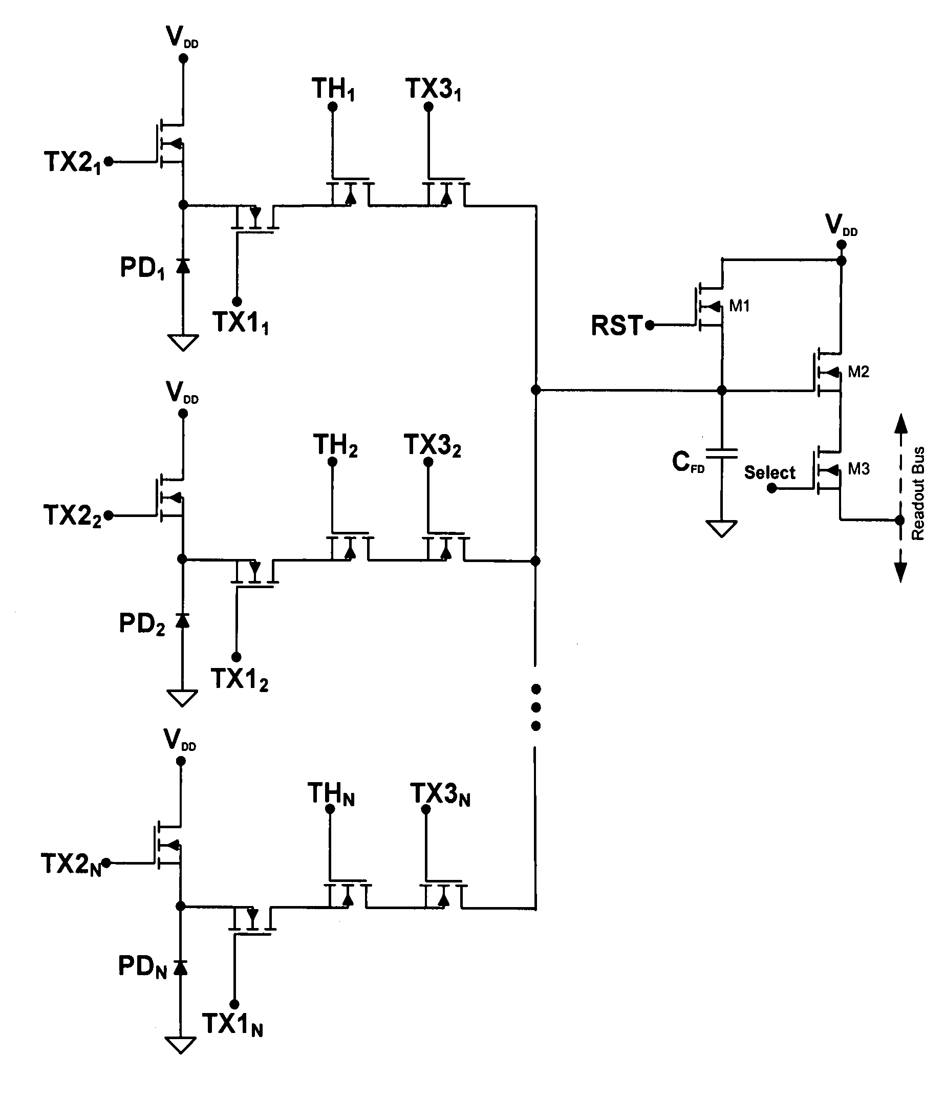
[0024]According to the present invention, a circuit supporting global shutter image formation, correlated double sampling, and transistor sharing is provided that reduces the average transistor per pixel count, while still being compatible with conventional CMOS image sensor (CIS) process technology.

[0025]An embodiment of the present invention is illustrated in FIG. 5. Each photodiode PDN has a circuit leg having its own reset transistor TX2, capture transistor TX1, hold transistor TH, and transfer transistor TX3. For convenience, the photodiode and related cir...


PUM


Abstract

A pixel circuit having a global shutter and transistor circuit sharing for CMOS image sensors. In one embodiment, a shared circuit includes a reset transistor, an amplifier transistor, and a readout transistor. At least two photodiode signal generation circuits share the shared circuit, wherein each signal generation circuit includes a capture transistor, a hold transistor, and a transfer transistor. Each pixel generation circuit may also include a photodiode reset transistor. In an alternate embodiment, each signal generation circuit does not include a separate transfer transistor, instead, the transfer transistor is part of the shared circuit.

Description

BACKGROUND OF THE INVENTION[0001]1. Field of the Invention[0002]The present invention relates generally to CMOS image sensors, and more particularly to global shutter pixel circuits sharing components between pixels.[0003]2. Description of the Related Art[0004]Visible imaging systems implemented using CMOS image sensors significantly reduce camera cost and power while improving resolution and reducing noise. The latest cameras use CMOS imaging System-on-Chip (iSoC) sensors that efficiently marry low-noise image detection and processing with a host of supporting blocks including timing controller, clock drivers, reference voltages, A / D conversion and key signal processing elements. High-performance video cameras are hence assembled using a single CMOS integrated circuit supported by only a lens and battery. These improvements translate into smaller camera size and longer battery life. The improvements also translate to the emergence of dual-use cameras that simultaneously produce hig...

Claims


Application Information

Patent Timeline
IPC IPC(8): H01L27/00
CPCH04N5/353H01L27/14641H04N5/37457H04N25/53H04N25/778
Inventor BLANQUART, LAURENT
Owner ALTASENS
Why Eureka
Try Eureka