Finfet memory device with dual separate gates and method of operation

a memory device and gate technology, applied in the field of semiconductor memory devices, can solve the problems of reducing scalability, increasing complexity while reducing scalability, and forming dual work function gates, so as to achieve the effect of enlarging or restricting the channel, enabling the change of channel conductivity, and reducing the cost of operation

Inactive Publication Date: 2009-04-30
IBM CORP
View PDF2 Cites 314 Cited by
  • Summary
  • Abstract
  • Description
  • Claims
  • Application Information

AI Technical Summary

Benefits of technology

[0002]The transistor is a solid state semiconductor device which can be used for amplification, switching, voltage stabilization, signal modulation and many other functions. Generally, a transistor has three terminals, and a voltage applied to a specific one of the terminals controls current flowing between the other two terminals.
[0003]The terminals of a field effect transistor (FET) are commonly named source, gate and drain. In the FET, a small amount of voltage is applied to the gate in order to control current flowing between the source and drain. In FETs, the main current appears in a narrow conducting channel formed near (usually primarily under) the gate. This channel connects electrons from the source terminal to the drain terminal. The channel conductivity can be altered by varying the voltage applied to the gate terminal, enlarging or constricting the channel and thereby controlling the current flowing between the source and the drain.
[0005]FIG. 1 illustrates a FET 100 comprising a p-type substrate (or a p-well in the substrate), and two spaced-apart n-type diffusion areas—one of which will serve as the “source”, the other of which will serve as the “drain” of the transistor. The space between the two diffusion areas is the “channel”. A thin dielectric layer is dispos...

Problems solved by technology

Embedded DRAM or DRAM is difficult to scale due to requirement of a large capacitor.
However, a back gate is required to modulate charge stored in the b...

Method used


Image

  • Finfet memory device with dual separate gates and method of operation
  • Finfet memory device with dual separate gates and method of operation
  • Finfet memory device with dual separate gates and method of operation

Examples


Embodiment Construction

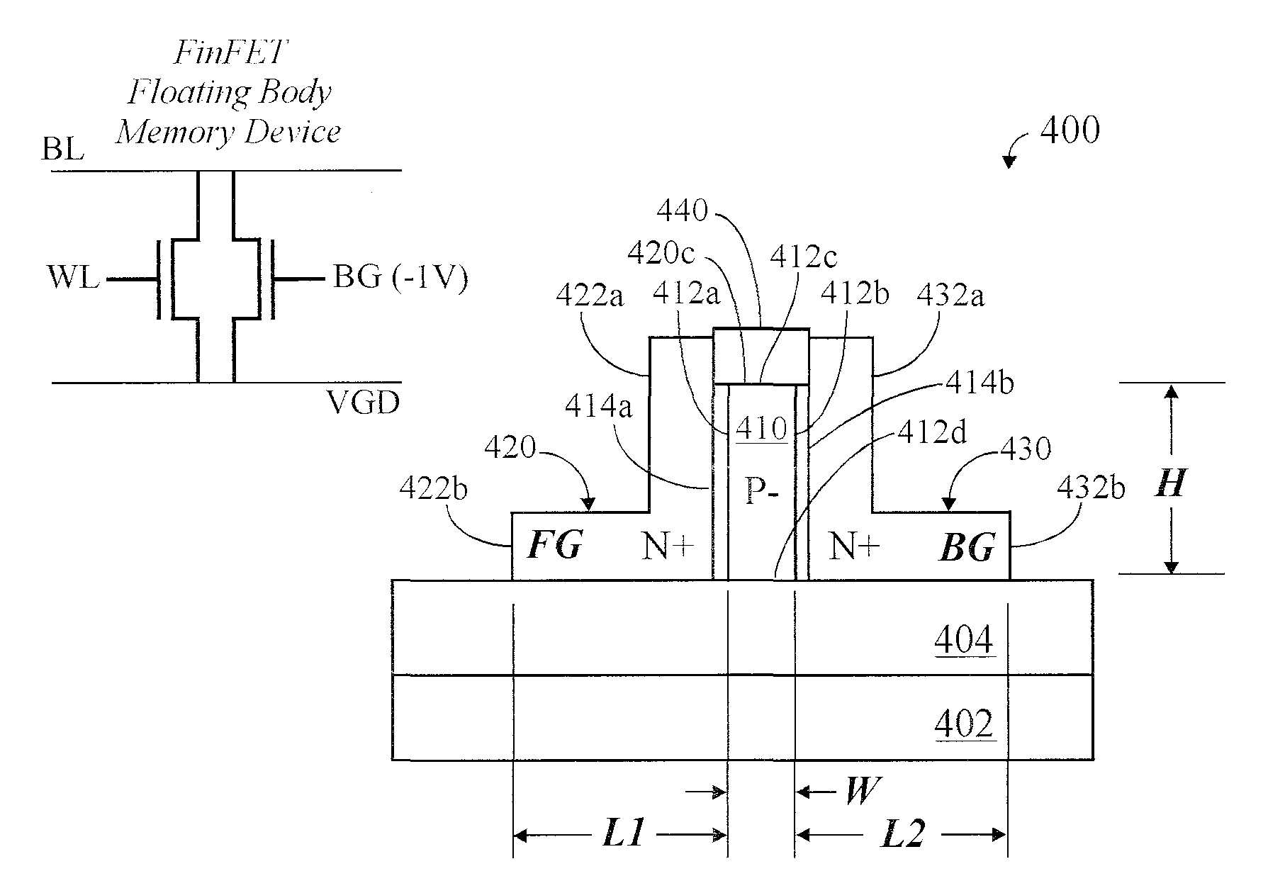
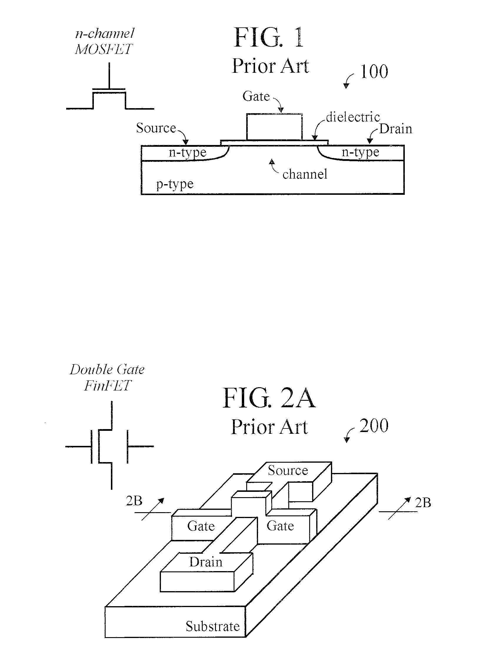
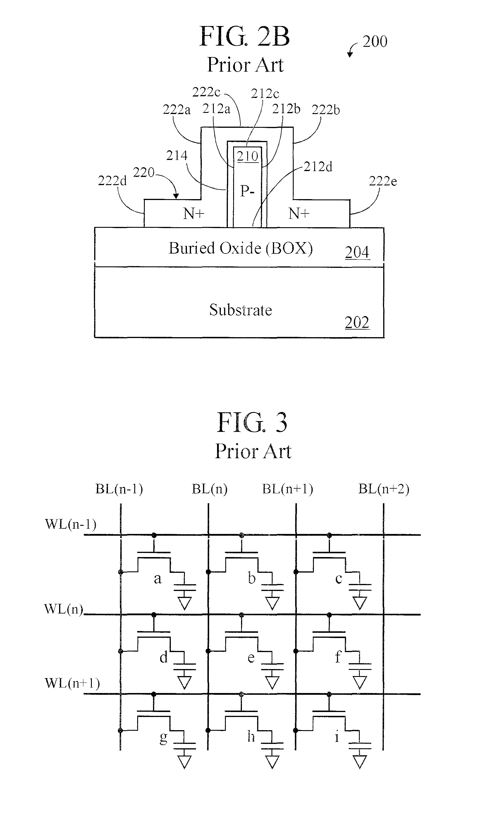
[0124]In the following detailed description, numerous specific details are set forth in order to provide a thorough understanding of the disclosure. However, it will be understood by those skilled in the art that the teachings of the present disclosure may be practiced without these specific details. In other instances, well-known methods, procedures, components and circuits have not been described in detail so as not to obscure the teachings of the present disclosure.

[0125]Materials (such as silicon dioxide) may be referred to by their formal and / or common names, as well as by their chemical formula. Regarding chemical formulas, numbers may be presented in normal font rather than as subscripts. For example, silicon dioxide may be referred simply as “oxide”, chemical formula SiO2.

[0126]In the description that follows, exemplary dimensions may be presented for an illustrative embodiment of the teachings of the disclosure. The dimensions should not be interpreted as limiting. They are...


PUM


Abstract

A FinFET device comprises a front gate (FG) and a separate back gate (BG) disposed on opposite sides of the fine. The fin structure may act as a floating body of a volatile memory cell. The front and back gates may be doped with the same or opposite polarity, and may be biased oppositely. A plurality of FinFETs may be connected in a memory array with single column erase, or double column erase capability.

Description

TECHNICAL FIELD[0001]The invention relates to the structure and operation of semiconductor memory cells, and more particularly to FinFET memory devices (or cells).BACKGROUND ARTThe Field Effect Transistor[0002]The transistor is a solid state semiconductor device which can be used for amplification, switching, voltage stabilization, signal modulation and many other functions. Generally, a transistor has three terminals, and a voltage applied to a specific one of the terminals controls current flowing between the other two terminals.[0003]The terminals of a field effect transistor (FET) are commonly named source, gate and drain. In the FET, a small amount of voltage is applied to the gate in order to control current flowing between the source and drain. In FETs, the main current appears in a narrow conducting channel formed near (usually primarily under) the gate. This channel connects electrons from the source terminal to the drain terminal. The channel conductivity can be altered by...

Claims


Application Information

Patent Timeline
IPC IPC(8): H01L29/786H01L27/12
CPCH01L27/108H01L27/10802H01L29/785H01L29/7841H01L27/10826H01L29/7855H10B12/20H10B12/00H10B12/36
Inventor YANG, HAINING S.WONG, ROBERT C.ZHU, HUILONG
Owner IBM CORP
Why Eureka
Try Eureka