Combination trim and CMFB circuit and method for differential amplifiers

Active Publication Date: 2009-04-30
TEXAS INSTR INC
View PDF6 Cites 8 Cited by
  • Summary
  • Abstract
  • Description
  • Claims
  • Application Information

AI Technical Summary

Benefits of technology

[0017]It is another object of the invention to provide a differential amplifier having both high speed common mode feedback and programmable input offset trim capability and which has substantially less complex circuitry and substantially lower noise than the closest prior art.
[0018]It is another object of the invention to provide a differential amplifier having both high speed common mode feedback and programmable input offset trim capability and which requires less integrated circuit chip area and which also reduces power consumption, while also providing increased speed and improved noise performance of the differential amplifier.

Problems solved by technology

These input offset compensation techniques require an additional differential input transistor pair and associated tail current source and also require a trim voltage generator circuit, and are characterized by undesirably high noise levels and undesirably high circuit complexity.
The prior art differential amplifiers having both high speed common mode feedback and programmable input offset trim capability require undesirably complex circuitry and an undesirably large amount of integrated circuit chip area, and are characterized by undesirably high noise levels associated with the connections of the common mode feedback circuitry and offset trim generators to the amplifier input stage and by undesirably high power consumption.

Method used


Image

  • Combination trim and CMFB circuit and method for differential amplifiers
  • Combination trim and CMFB circuit and method for differential amplifiers
  • Combination trim and CMFB circuit and method for differential amplifiers

Examples


Embodiment Construction

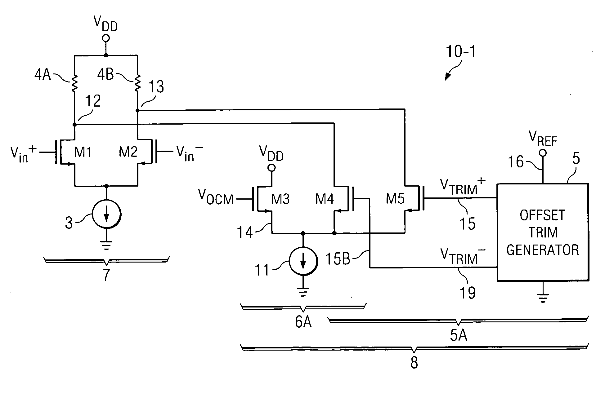
[0031]Referring to FIG. 3, single-stage differential amplifier 10-1 includes an input stage 7 including N-channel input transistors M1 and M2 having their sources connected to a tail current source 3. The gates of input transistors M1 and M2 are coupled to Vin+ and Vin−, respectively. The drain of input transistor M1 is connected by conductor 12 to one terminal of load resistor 4A, and the drain of input transistor M2 is connected by conductor 13 to one terminal of load resistor 4B. The upper terminals of load resistors 4A and 4B are connected to supply voltage VDD.

[0032]In accordance with the present invention, single-stage differential amplifier 10-1 also includes a combined common mode feedback and input offset adjustment circuit 8 (referred to herein as “combined CMFB and offset adjustment circuit 8”). Combined CMFB and offset adjustment circuit 8 includes an input offset adjustment section 5A and a common mode feedback section 6A. Conductor 12 is connected to the drain of N-cha...


PUM


Abstract

A differential amplifier (10-1,2) includes an input stage (7) including first (M1) and second (M2) input transistors and first (4A) and second (4B) load devices. Sources of the first and second input transistors are connected together. Drains of the first and second input transistors are coupled by first (12) and second (13) conductors to the first and second load devices, respectively. Common mode feedback circuitry (6A) including first (M3), second (M4), and third (M5) transistors is combined with offset correction circuitry (8) including the second transistor and the third transistor. Sources of the first, second, and third transistors are coupled to a tail current source (11). Drains of the second and third transistors are coupled to the first and second conductors, respectively. A common mode voltage (VOCM) is applied to a gate of the first transistor. Offset trim voltages are applied to gates of the second and third transistors.

Description

CROSS REFERENCE TO RELATED APPLICATION[0001]This application claims the benefit of prior filed co-pending U.S. provisional application Ser. No. 60 / 984,200 filed Oct. 31, 2007, entitled “COMBINATION TRIM & CMFB CIRCUIT FOR DIFFERENTIAL AMPLIFIERS”, by Brett Forejt, and incorporated herein by reference.BACKGROUND OF THE INVENTION[0002]The present invention relates generally to integrated circuit differential amplifiers having high speed common mode feedback and also having programmable input offset trim capability, and more particularly to improvements which result in substantially reduced circuit complexity and substantially reduced noise levels.[0003]In the prior art, there are several ways to accomplish input offset compensation, for example by trimming or calibrating load devices of the input stage or by injecting an offset compensation current into the circuit nodes between drains of the input transistors and their corresponding load devices. These input offset compensation techn...

Claims


Application Information

Patent Timeline
IPC IPC(8): H03F3/45
CPCH03F3/45183H03F3/45632H03F2203/45048H03F2203/45702H03F2203/45438H03F2203/45678H03F2203/45681H03F2203/45436
Inventor FOREJT, BRETT E.
Owner TEXAS INSTR INC
Why Eureka
Try Eureka