Liquid crystal display device

a liquid crystal display and display device technology, applied in the field of display devices, can solve the problems of difficult to form a black matrix on the tft substrate, and achieve the effects of reducing the number of components, increasing the reliability of the connection portion, and maintaining the contrast of an imag

Active Publication Date: 2009-05-07
JAPAN DISPLAY INC
View PDF1 Cites 63 Cited by
  • Summary
  • Abstract
  • Description
  • Claims
  • Application Information

AI Technical Summary

Benefits of technology

[0014]An object of the invention is to enable a structure in which, in a liquid crystal display device using the capacitive touch screen 50, the touch screen 50 is installed on the color filter substrate 20 side of the liquid crystal display device. Also, another object of the invention is to connect the liquid crystal panel and the touch screen 50 with the same flexible wiring substrate 70, reducing a number of components of a connection portion. Also, yet another object of the invention is to realize a compact liquid crystal display device with touch screen.
[0021]According to the invention, as it is possible to install the touch screen on the color filter substrate side of the liquid crystal display panel, it is possible to maintain the contrast of an image. Also, according to the invention, as the connection portion of the touch screen and flexible wiring substrate, as well as the connection portion of the liquid crystal display panel and flexible wiring substrate, are installed on the interior side, it is possible to increase a reliability of the connection portion. Also, as it is possible to share the flexible wiring substrate connected to the touch screen and the liquid crystal display panel, it is possible to reduce the number of components.
[0022]Furthermore, according to the invention, as the substrate of the touch screen is disposed on an exterior side, it is possible to protect the wiring of the touch screen. Furthermore, according to the invention, as it is possible to reduce a bending stress of the flexible wiring substrate, it is possible to realize a compact liquid crystal display device with touch screen.

Problems solved by technology

Another problem with the configuration shown in FIG. 11 is as follows.
That is, although it is possible to form a black matrix in order to raise the contrast on a color filter substrate 20 side, it is difficult to form a black matrix on the TFT substrate 10 side.

Method used


Image

  • Liquid crystal display device
  • Liquid crystal display device
  • Liquid crystal display device

Examples


first embodiment

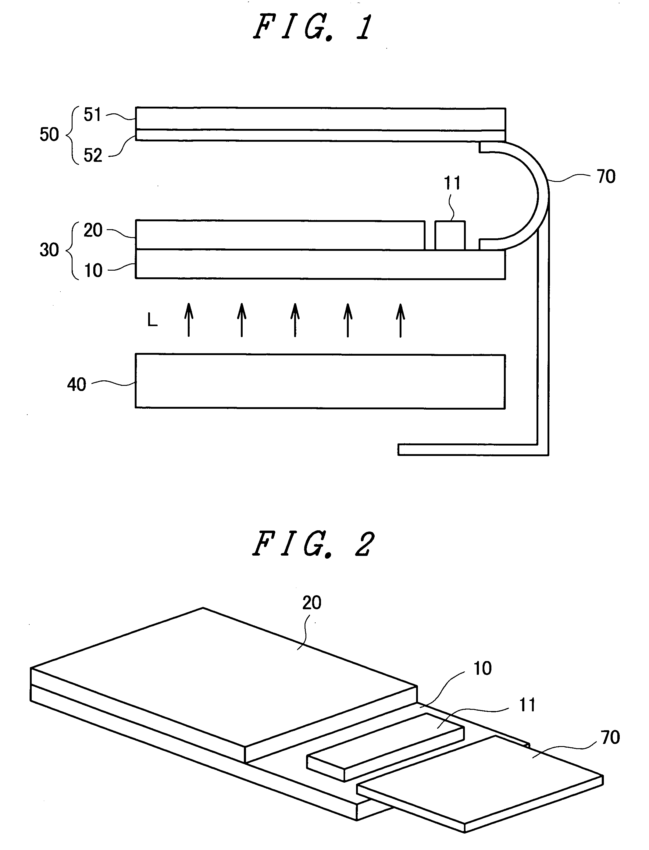
[0035]FIG. 1 is a schematic sectional view of a liquid crystal display device with touch screen according to the invention.

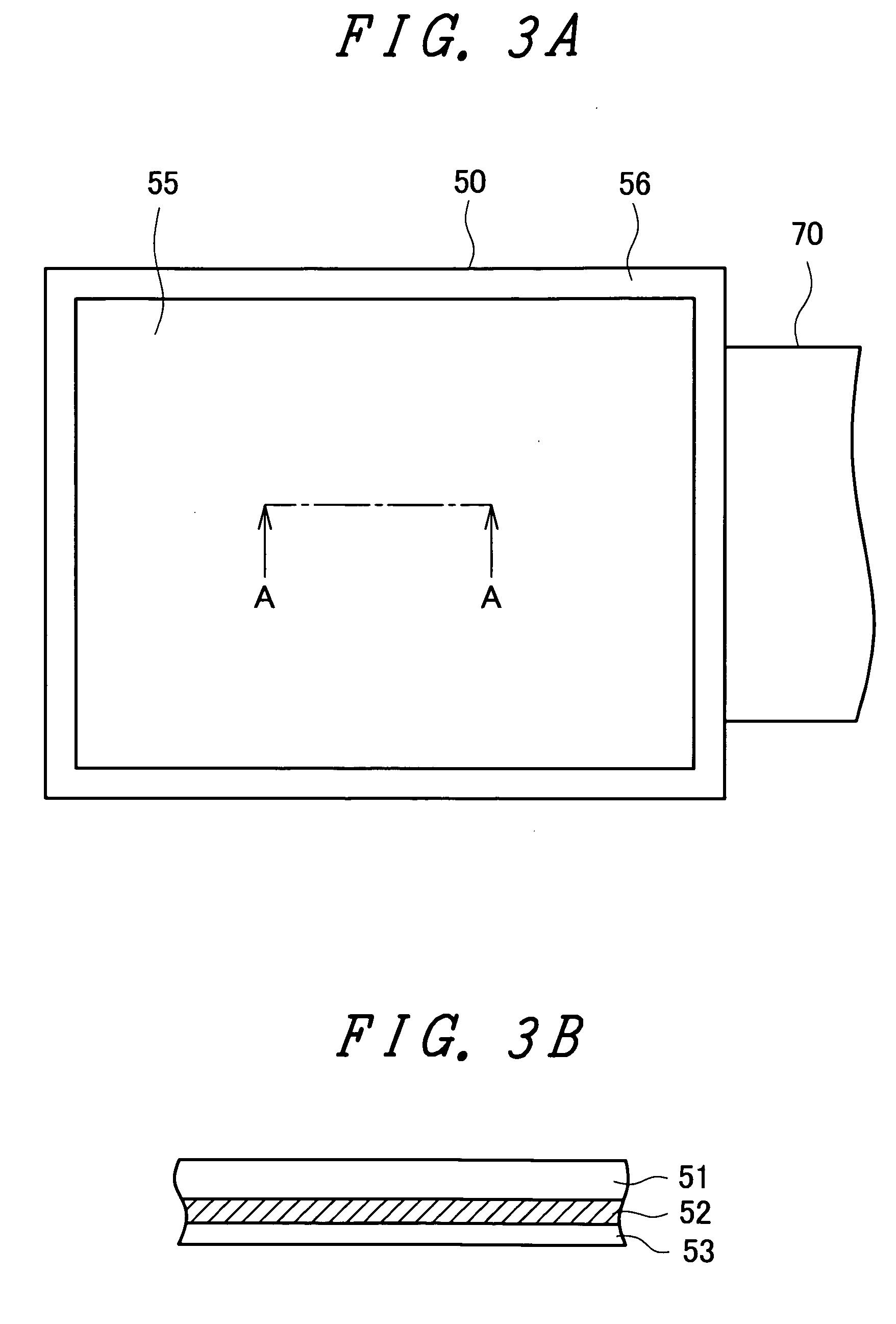
[0036]A touch screen 50 in the embodiment is a static capacitance coupling type of touch screen (hereafter called a capacitive touch screen) 50. An outline structure of the capacitive touch screen (the touch panel) 50 is that a conductive layer 52, configuring one portion of a position detection circuit, is formed on a transparent touch screen substrate 51. Although not shown in FIG. 1, the conductive layer 52 is covered with a protection layer.

[0037]One feature of the embodiment is that a surface touched with a human finger, or with a pen or the like, is a surface on a side opposite to a surface of the touch screen substrate on which the conductive layer 52 is formed. In the case of many capacitive touch screens 50, a human touches the conductive layer 52 side. Although the conductive layer 52 is covered with a protection layer, the protection layer tears on be...

second embodiment

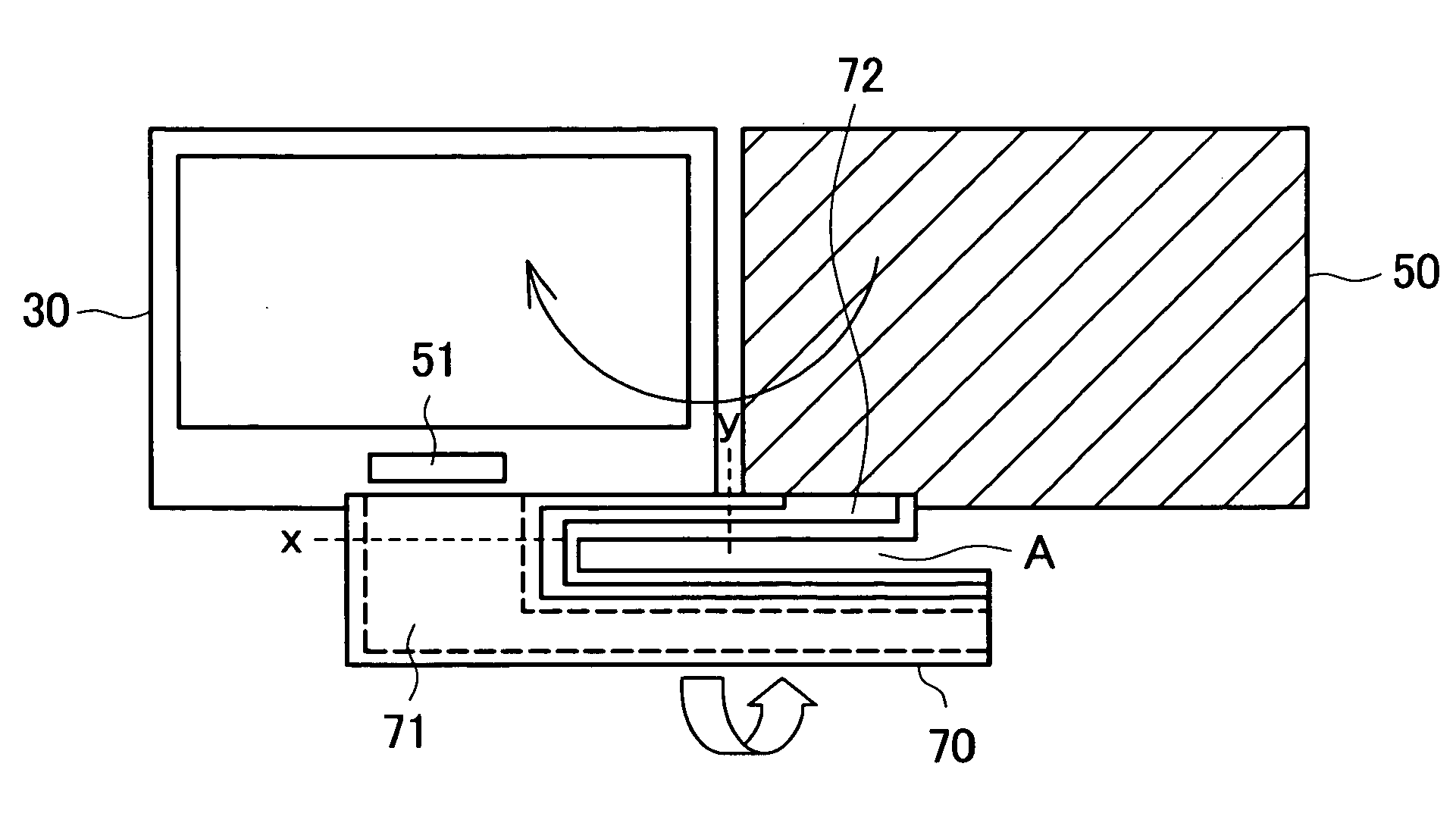
[0058]FIGS. 6A and 6B are a second embodiment of the invention. FIG. 6A is a plan view of the liquid crystal display panel 30 and the touch screen 50 before stacking, while FIG. 6B is a plan view of the liquid crystal display panel 30 and the touch screen 50 after stacking. In the flexible wiring substrate 70 of FIG. 6A, the wiring for the liquid crystal display panel 30 is formed on a rear side, and the wiring for the touch screen 50 on a front side.

[0059]In FIG. 6A, firstly, the flexible wiring substrate 70 is folded along the dashed line y, and the liquid crystal display panel 30 and touch screen 50 are laid one on top of the other. At this time, only a narrow portion of the flexible wiring substrate 70, in which only the wiring for the touch screen 50 is formed, is folded. Consequently, the bending stress is small.

[0060]After the liquid crystal display panel 30 and touch screen 50 are laid one on top of the other, the flexible wiring substrate 70 is folded to the rear of the liq...

third embodiment

[0063]FIGS. 7A, 7B and 7C are a third embodiment of the invention.

[0064]FIG. 7A is a plan view of the liquid crystal display panel 30 and the touch screen 50 before stacking, FIG. 7B is a plan view of the liquid crystal display panel 30 and the touch screen 50 after stacking, and FIG. 7C is a plan view after folding the flexible wiring substrate 70 to the rear side of the liquid crystal display panel 30. In the flexible wiring substrate 70 of FIG. 7A, the wiring for the liquid crystal display panel 30 and the wiring for the touch screen 50 are formed on the same surface side. Furthermore, the flexible wiring substrate 70 is connected to a front surface side of the liquid crystal display panel 30 and a rear surface side of the touch screen 50. The front surface is called an observer side, while the rear surface is called a backlight side.

[0065]In FIG. 7A, the liquid crystal display panel 30 and touch screen 50 are laid one on top of the other by folding the flexible wiring substrate ...


PUM


Abstract

To realize an increase in an image quality of a liquid crystal display device having a capacitive touch screen, and an increase in a reliability of a contact surface and a connection portion.A capacitive touch screen 50 and a liquid crystal display panel 30 are connected, by the same flexible wiring substrate 70, on an interior side when the touch screen 50 and the liquid crystal display panel 30 are laid one on top of the other. By so doing, a terminal is protected from an exterior, and an increase in a number of components is suppressed. Also, by installing the capacitive touch screen 50 on a color filter substrate 20 side of the liquid crystal display panel 30, a reduction of a contrast is prevented. Furthermore, a capacitive touch screen substrate 51 side is made a contact surface for an input. By so doing, a conductive layer 52 of the capacitive touch screen 50 is prevented from tearing due to an abrasion caused by a contact.

Description

CROSS-REFERENCE TO RELATED APPLICATION[0001]The present application claims priority from Japanese application JP2007-289740 filed on Nov. 7, 2007, the content of which is hereby incorporated by reference into this application.BACKGROUND OF THE INVENTION[0002]1. Technical Field[0003]The present invention relates to a display device, and particularly relates to a liquid crystal display device having a touch screen.[0004]2. Related Art[0005]As a liquid crystal display device can be made compact and slimline, applications are expanding into various fields. A mobile telephone, a PDA, and the like, are examples thereof. In these apparatus, a method wherein a touch screen is used as an input device is expanding. Although there is a static capacitance coupling type, a resistance type, and the like, of touch screen, a configuration in which a resistance type touch screen is used as an input device of a liquid crystal display device is described in JP-A-2005-38231.[0006]In JP-A-2005-38231, a ...

Claims


Application Information

Patent Timeline
Patent Type & Authority Applications(United States)
IPC IPC(8): G06F3/045
CPCG06F3/044G06F3/0412G06F3/0444G06F3/04164
Inventor OOWAKI, YOSHIO
Owner JAPAN DISPLAY INC
Why Eureka
Try Eureka