Front-Illuminated Avalanche Photodiode

Active Publication Date: 2009-05-14
LUMENTUM OPERATIONS LLC
View PDF1 Cites 41 Cited by
  • Summary
  • Abstract
  • Description
  • Claims
  • Application Information

AI Technical Summary

Benefits of technology

[0019]Accordingly, the present invention relates to a front-illuminated avalanche photodiode (APD) comprising: an APD body of semiconductor material, including: a substrate; and a layer stack, disposed on a front surface of the substrate, comprising: an absorption layer for absorbing light at an absorption wavelength band to generate a photocurrent; a multiplication layer, including a multiplication region, for multiplying the photocurrent through avalanche multiplication; and a field-control layer for controlling electric fields in the absorption layer and the multiplication layer; wherein a back surface of the APD body is mechanically and chemically polished; and a reflector having a reflectance of greater than 90% at the absorption wavelength band, for reflecting light at the absorption wavelength band toward the absorption layer, disposed on the back surface of the APD body.
[0020]Anot

Problems solved by technology

However, the formation of a DBR of semiconductor material with a high reflectivity is challenging and adds complexity to the manufacturing process of the front-illuminated APDs.
However, the manufacturing yield of back-illuminated APDs is relatively low, because, typical

Method used


Image

  • Front-Illuminated Avalanche Photodiode
  • Front-Illuminated Avalanche Photodiode
  • Front-Illuminated Avalanche Photodiode

Examples


first embodiment

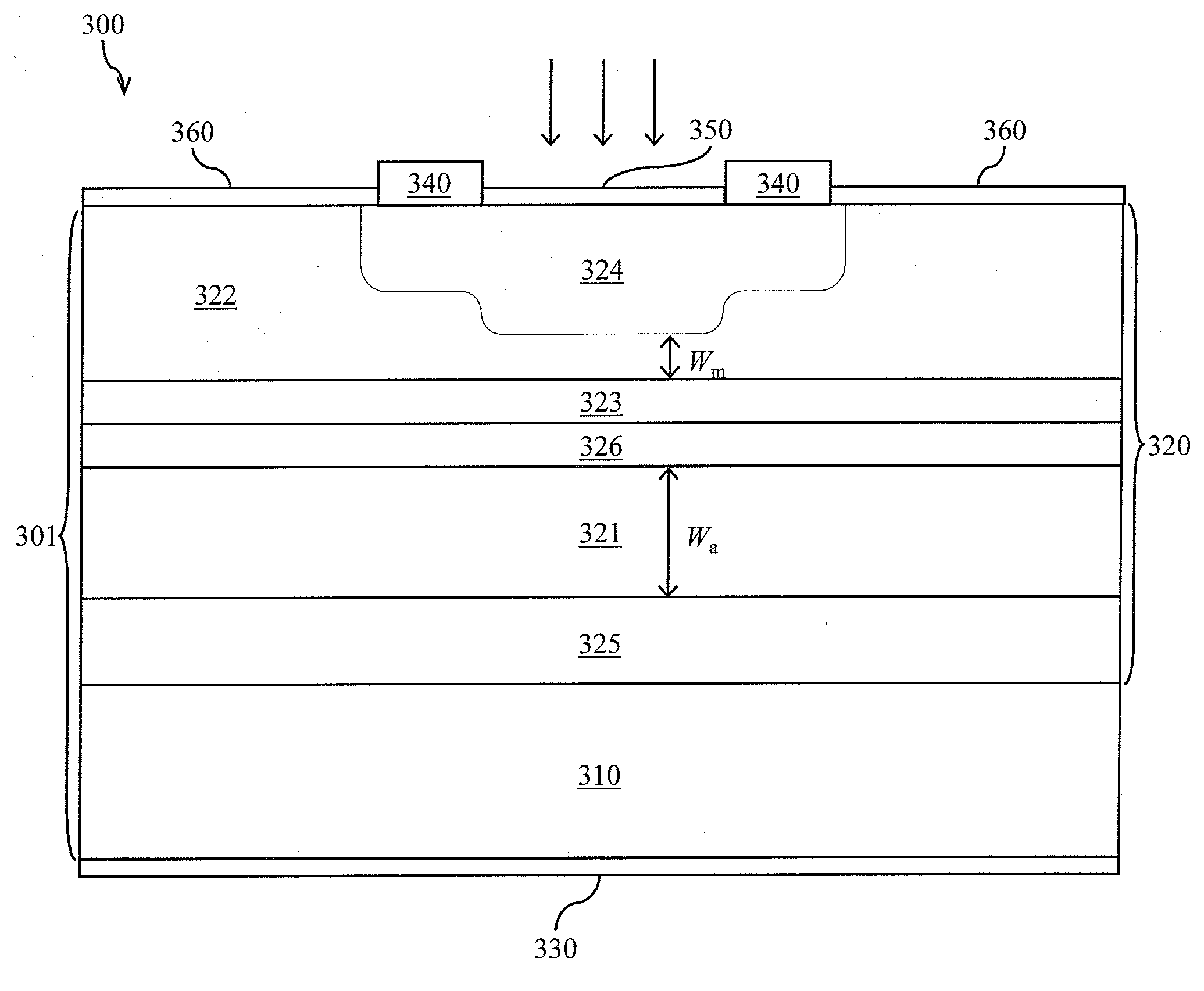
[0035]With reference to FIG. 3, a front-illuminated APD 300 includes an APD body 301 of semiconductor material, which has a layer structure similar to that of the prior-art APD body 101. The APD body 301 includes a substrate 310 and a layer stack 320. Advantageously, a back surface of the APD body 301 is mechanically and chemically polished to increase a reflectance of the back surface of the APD body 301 at an absorption wavelength band.

[0036]The layer stack 320 comprises an absorption layer 321, for absorbing light at the absorption wavelength band to generate a photocurrent, a multiplication layer 322, which includes a multiplication region, for multiplying the photocurrent through avalanche multiplication, and a field-control layer 323, for controlling electric fields in the absorption layer 321 and the multiplication layer 322. The multiplication layer 322 includes a diffusion region 324, for defining the multiplication region and for providing a p-n junction. In some instances...

second embodiment

[0053]With reference to FIG. 4, a front-illuminated APD 400 includes an APD body 401, which has a layer structure similar to that of the prior-art APD body 201. The APD body 401 includes the substrate 310 of the front-illuminated APD 300, as well as a layer stack 420. Advantageously, a back surface of the APD body 401 is mechanically and chemically polished to increase a reflectance of the back surface of the APD body 401 at the absorption wavelength band.

[0054]The layer stack 420 comprises the absorption layer 321 and the buffer layer 325 of the front-illuminated APD 300. The layer stack 420 further comprises a multiplication layer 422, which includes a multiplication region, for multiplying the photocurrent through avalanche multiplication, a field-control layer 423, for controlling electric fields in the absorption layer 321 and the multiplication layer 422, and a window layer 427, for transmitting light at the absorption wavelength band to the absorption layer 321. The window la...

third embodiment

[0062]With reference to FIG. 5, a front-illuminated APD 500 includes the APD body 301, the front contact 340, the antireflection layer 350, and the passivation layer 360 of the front-illuminated APD 300. In addition, the front-illuminated APD 500 includes a reflector 530 having a reflectance of greater than 90% at the absorption wavelength band, for reflecting light at the absorption wavelength band toward the absorption layer 321, as well as a back contact 570 of metallic material, for passing current to or from the front-illuminated APD 500.

[0063]The back contact 570 is annular and is disposed on an annular contact region of the back surface of the APD body 301, such that an inner circumference of the back contact 570 defines a circular reflector region of the back surface of the APD body 301. The reflector 530 is disposed on the reflector region of the back surface of the APD body 301. Preferably, the reflector 530 is disposed only on the reflector region of the back surface of t...


PUM


Abstract

The present invention provides a front-illuminated avalanche photodiode (APD) with improved intrinsic responsivity, as well as a method of fabricating such a front-illuminated APD. The front-illuminated APD comprises an APD body of semiconductor material, which includes a substrate and a layer stack disposed on a front surface of the substrate. The layer stack includes an absorption layer, a multiplication layer, and a field-control layer. Advantageously, a back surface of the APD body is mechanically and chemically polished, and a reflector having a reflectance of greater than 90% at the absorption wavelength band is disposed on the back surface of the APD body. Thus, incident light that is not absorbed in a first pass through the absorption layer is reflected by the reflector for a second pass through the absorption layer, increasing the intrinsic responsivity of the front-illuminated APD.

Description

CROSS-REFERENCE TO RELATED APPLICATIONS[0001]The present invention claims priority from U.S. Patent Application No. 60 / 987,878 filed Nov. 14, 2007, which is incorporated herein by reference.TECHNICAL FIELD[0002]The present invention relates to avalanche photodiodes (APDs) and, in particular, to front-illuminated APDs.BACKGROUND OF THE INVENTION[0003]In optical communication systems, avalanche photodiodes (APDs) are used to convert optical signals into electrical signals. APDs having a planar configuration are among the most reliable. With reference to FIGS. 1 and 2, a typical planar APD comprises an APD body 101 or 201 of semiconductor material, as disclosed in U.S. Pat. No. 6,515,315 to Itzler, et al., issued on Feb. 4, 2003; and in U.S. Patent Application Publication No. 2008 / 0121867 to Yagyu, et al., published on May 29, 2008; respectively, which are incorporated herein by reference.[0004]The APD body 101 or 201 includes a substrate 110 or 210 and a layer stack 120 or 220, dispos...

Claims


Application Information

Patent Timeline
IPC IPC(8): H01L31/107H01L31/18
CPCH01L31/18H01L31/107
Inventor PAN, ZHONGCIESLA, CRAIG
Owner LUMENTUM OPERATIONS LLC
Why Eureka
Try Eureka