Image processing apparatus and image processing apparatus controlling method

a technology of image processing apparatus and control method, which is applied in the direction of visual presentation, instruments, camera body details, etc., can solve the problems of insufficient power consumption reduction arrangement, inability to bring its operating frequency under a given lower frequency limit, and difficulty in keeping the power dissipation of memory units low enough, so as to minimize power dissipation

Inactive Publication Date: 2009-05-14
SONY CORP
View PDF2 Cites 11 Cited by
  • Summary
  • Abstract
  • Description
  • Claims
  • Application Information

AI Technical Summary

Benefits of technology

[0011]The present invention has been made in view of the above circumstances and provides an image processing apparatus and an image processing apparatus controlling method, the image processing apparatus utilizing general-purpose memory units to process pixel data coming from an imaging device while minimizing power dissipation, the processed pixel data being output to the outside.

Problems solved by technology

However, such arrangements are becoming insufficient in bringing down power consumption.
Even if there is a surplus bandwidth capacity for access to this type of memory unit, it is impossible to bring its operating frequency under a given lower frequency limit.
This makes it difficult to keep the power dissipation of the memory units low enough.
One disadvantage of the disclosed apparatus is that it needs a traffic monitoring device when configured.
Another disadvantage is that delays in bus width changeover are bound to occur because the process of data traffic monitoring precedes the operation of bus width changeover in the apparatus.
The latter disadvantage in particular makes it difficult for the cited bus control apparatus to keep up with rapid ups and downs in data traffic.
Moreover, the disclosed techniques are irrelevant to stopping the clock feed to part of the memory arrays or partially halting power supply to the memory arrays.
Furthermore, the proposed techniques above for changing memory array mapping are not shown applicable to inexpensive, common memory units such as SDRAMs (synchronous dynamic random access memory), DDR-SDRAMs (double-data-rate synchronous dynamic random access memory) and DDR2-SDRAMs.
In other words, these techniques are not available on the cheap.

Method used


Image

  • Image processing apparatus and image processing apparatus controlling method
  • Image processing apparatus and image processing apparatus controlling method
  • Image processing apparatus and image processing apparatus controlling method

Examples


Embodiment Construction

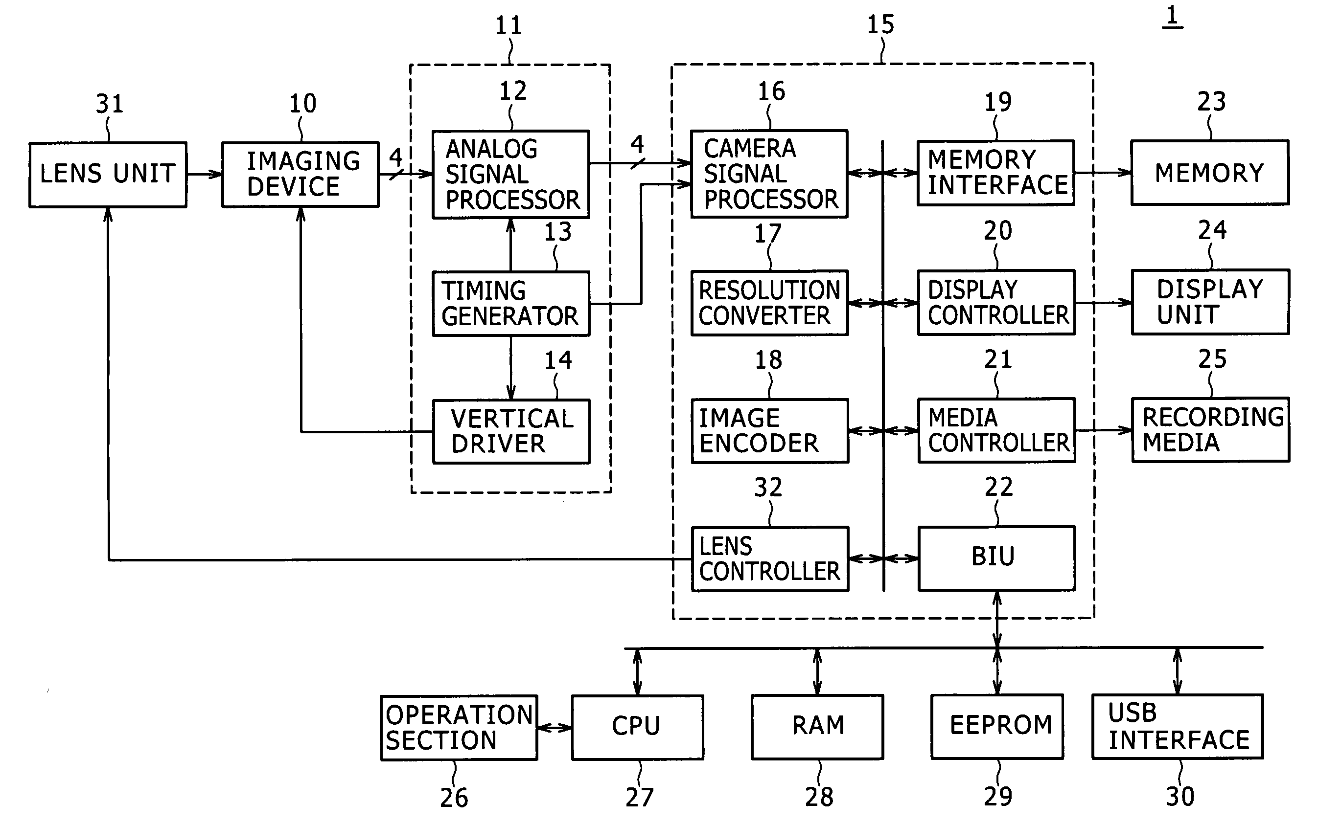
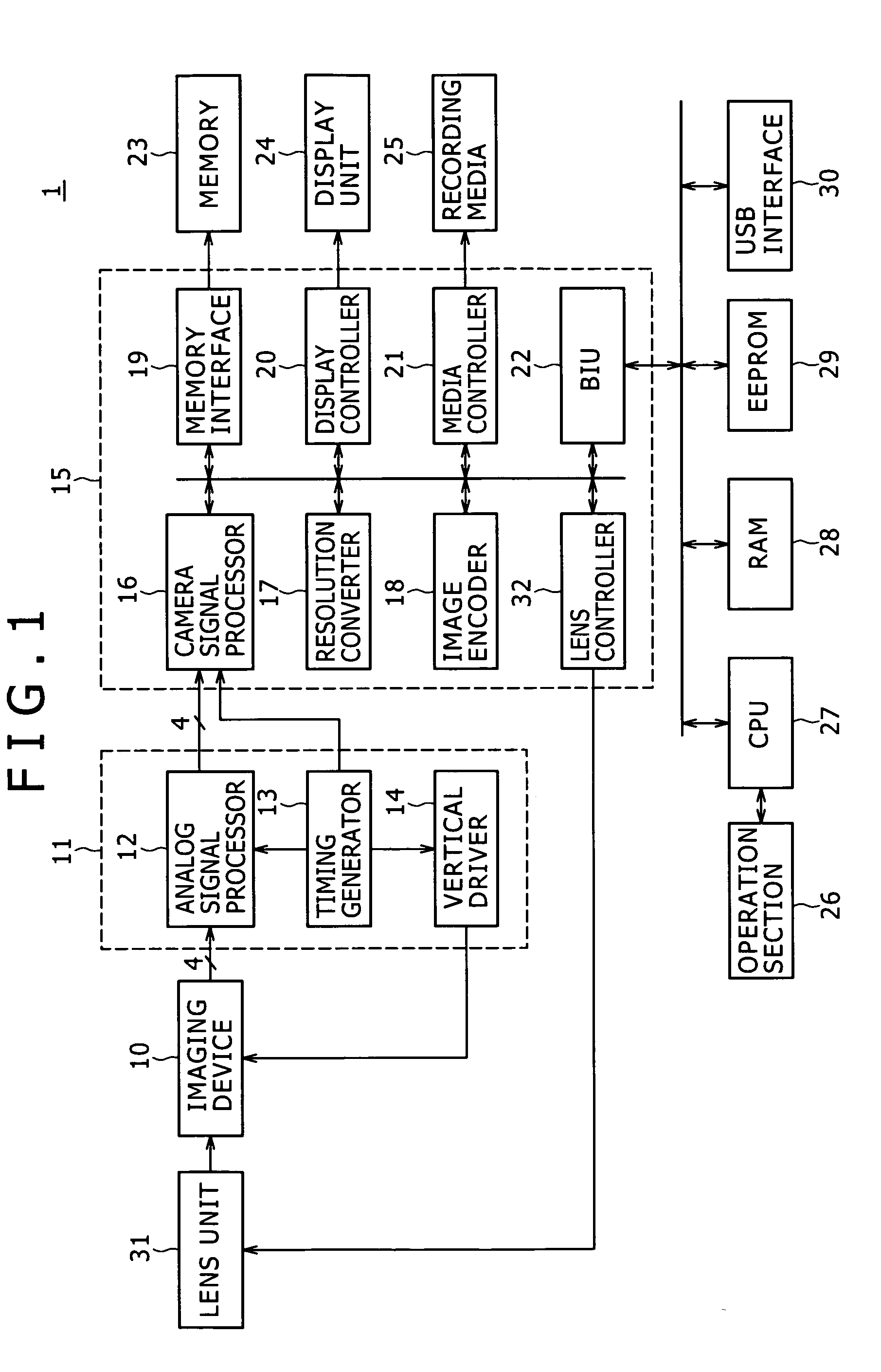
[0029]The image processing apparatus according to embodiments of the present invention is basically an apparatus that performs image processing on the pixel data acquired by an imaging device through the use of memory units. The ensuing description will focus illustratively on a digital camera 1 that images objects using a solid-state imaging device such as one shown in FIG. 1.

[0030]As indicated in FIG. 1, the digital camera 1 includes a lens unit 31, an imaging device 10, a preprocessor 11, an image processing device 15, a memory 23, a display unit 24, recording media 25, an operation section 26, a CPU (central processing unit) 27, a RAM (random access memory) 28, an EEPROM (electrically erasable and programmable read only memory) 29, and a USB (universal serial bus) interface 30.

[0031]The lens unit 31 includes a focusing lens, a zoom lens, an aperture mechanism, and drivers that drive these components in accordance with drive control signals fed by a lens controller 32, to be disc...


PUM


Abstract

Disclosed herein is an image processing apparatus including an input section, a bus, a memory interface, an output section, and a control section.

Description

CROSS REFERENCES TO RELATED APPLICATIONS[0001]The present invention contains subject matter related to Japanese Patent Application JP 2007-295967 filed in the Japan Patent Office on Nov. 14, 2007, the entire contents of which being incorporated herein by reference.BACKGROUND OF THE INVENTION[0002]1. Field of the Invention[0003]The present invention relates to an image processing apparatus for processing image data taken by an imaging device and a method for controlling such an image processing apparatus.[0004]2. Description of the Related Art[0005]Some solid-state imaging devices proposed in recent years are designed to output data constituting a plurality of pixels in serial form, in such a manner that the pixels were output individually and in parallel. Such imaging devices are disclosed illustratively by Japanese Patent Laid-Open Nos. 2005-86224 and 2005-244709. These solid-state imaging devices make it easy to change the number of parallelly output pixels. Illustratively, the nu...

Claims


Application Information

Patent Timeline
Patent Type & Authority Applications(United States)
IPC IPC(8): G06F3/00
CPCG03B17/00G06F1/3225G06F1/3203
Inventor YOKOYAMA, TOMONORI
Owner SONY CORP
Why Eureka
Try Eureka