Apparatus and method for producing electrically conducting nanostructures by means of electrospinning

a technology of electrical conductivity and electrospinning, applied in the direction of coating, filament/thread forming, fibre treatment, etc., can solve the problems of inability to achieve optical transparency and gloss in this connection, inability to achieve optical transparency and gloss in general, and inability to achieve optical transparency and gloss in practi

Inactive Publication Date: 2009-05-21
BAYER MATERIALSCIENCE AG
View PDF8 Cites 37 Cited by
  • Summary
  • Abstract
  • Description
  • Claims
  • Application Information

AI Technical Summary

Problems solved by technology

In particular the optical transparency and gloss are in this connection technically demanding.
Either the substrate material itself is specifically made electrically conducting, without thereby adversely affecting its mechanical and optical properties, or a material is used that is conducting but is not visually recognisable by the human eye and can easily be applied in a targeted manner to the surface of the substrate, or a conducting material is used, which although itself is not transparent, can however be applied by means of a suitable process to the surface in such a way that the resulting structure is in general not perceivable by the human eye without the assistance of optical aids.
However, this is not feasible in practice since with increasing reduction of the nozzle diameter the requirements on the inks that can be used become much more stringent.
In many cases these parameters cannot however be adjusted separately from the behaviour (e.g. spreading and adherence) of the ink on the respective substrate, which means that the ink and printing method combination cannot be used to produce conducting structures in this size range.
The disadvantage of hot stamping however is that the structural shape is restricted to the shape of the stamping punch or stamping roller that is used in each case.
A free choice in the configuration of the structure is not possible with this method.

Method used


Image

  • Apparatus and method for producing electrically conducting nanostructures by means of electrospinning
  • Apparatus and method for producing electrically conducting nanostructures by means of electrospinning

Examples


example 1

Conducting Nanostructures with Carbon Nanotubes

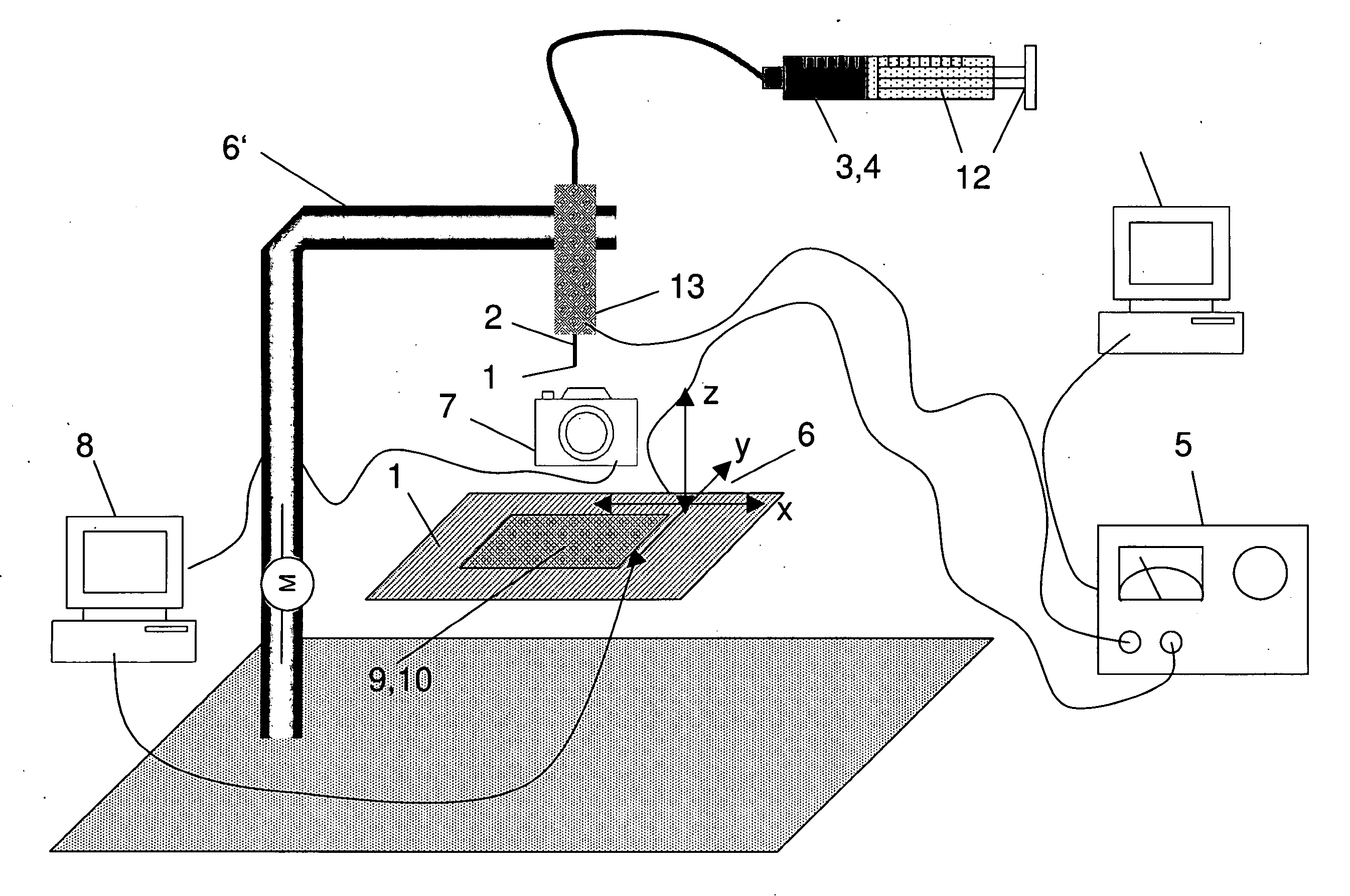
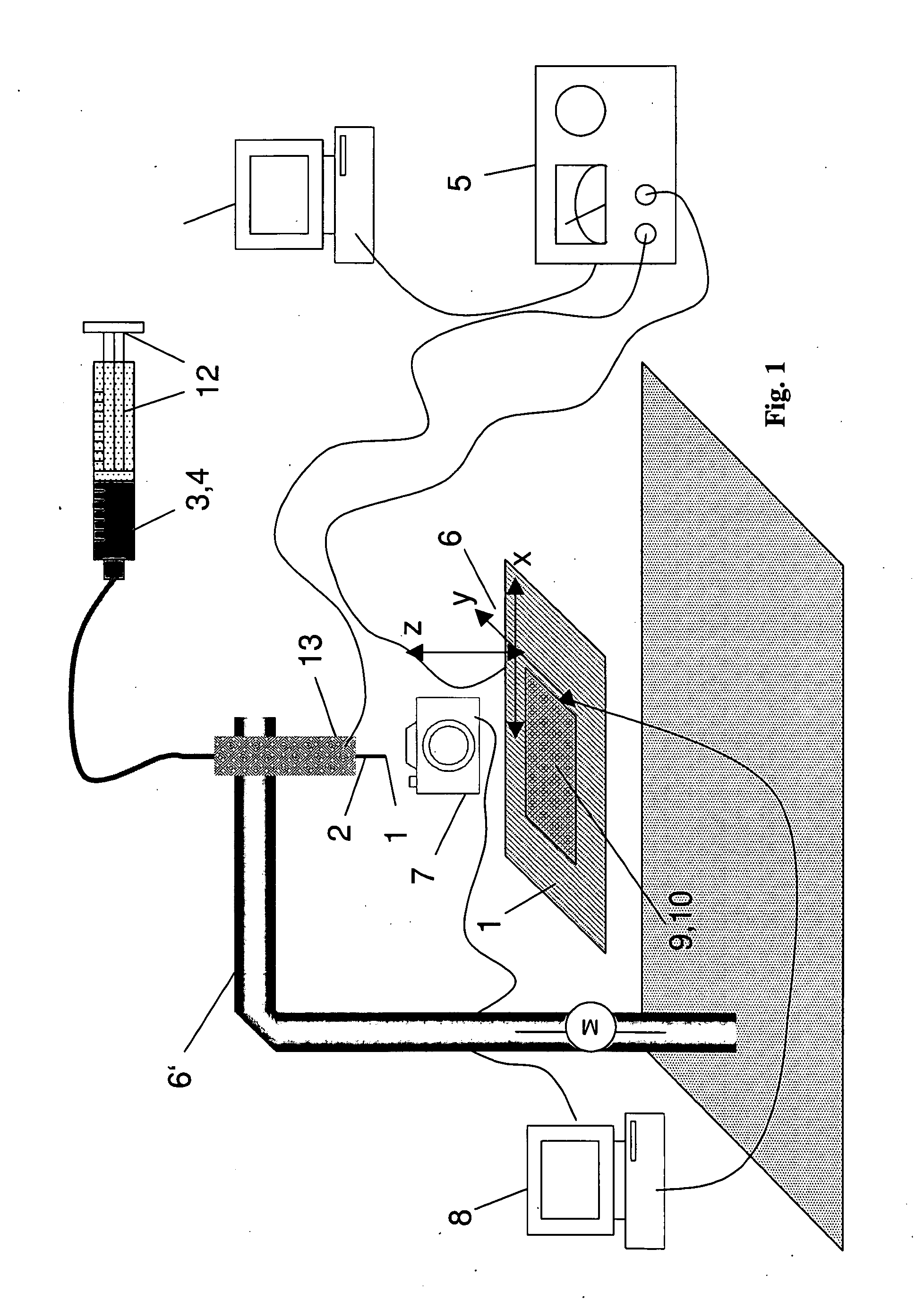
[0050]The following apparatus (see FIG. 1) was used for spinning the spinning solution:

[0051]The holder 1 for the substrate 9, which is a silicon disc, and the metallic holder 13 for the spinning capillary 2, which is provided with a liquid reservoir 3 for the spinning solution 4 and is connected to an electrical voltage supply 5. The voltage source 5 supplies D.C. voltage up to 10 kV. The spinning capillary 2 is a glass capillary with an internal diameter of 100 Mm. The controllable adjustment motor 6 serves to move the spinning capillary 2 and the adjustment motor 6′ serves to move the substrate holder 1 relative to one another so as to adjust the distance between them. The camera 7 is trained on the outlet of the spinning capillary 2 so as to follow the spinning procedure and is connected to a computer 8 with image processing software for evaluating the image data provided by the camera. The drive of the motor 6′ of the substrate hol...


PUM

PropertyMeasurementUnit
widthaaaaaaaaaa
widthaaaaaaaaaa
internal diameteraaaaaaaaaa

Abstract

Apparatus and method for producing electrically conducting nanostructures by means of electrospinning, the apparatus having at least a substrate holder (1), a spinning capillary (2), connected to a reservoir (3) for a spinning liquid (4) and to an electrical voltage supply (5), an adjustable movement unit (6, 6′) for moving the spinning capillary (2) and / or the substrate holder (1) relative to one another, an optical measuring device (7) for monitoring the spinning procedure at the outlet of the spinning capillary (2), and a computer unit (8) for controlling the drive of the spinning capillary (2) relative to the substrate holder (1) in accordance with the spinning procedure.

Description

[0001]The present invention starts from known methods for the production of structures of electrically conducting material using printing methods. The invention relates to a method by means of which it is possible to deposit nanofibres in a targeted manner with a high spatial precision onto any desired surface. This is made possible by a specially adapted process of so-called electrospinning in conjunction with a material suitable for this purpose, from which the electrically conducting structures are formed, wherein the structures consist of electrically conducting particles or are subjected to a post-treatment in order to impart conductivity.BACKGROUND OF THE INVENTION[0002]Many structural parts (e.g. many internal fittings of automobiles; discs) and objects of daily use (e.g. beverage bottles) consist substantially of electrically insulating materials. This includes known polymers, such as polyvinyl chloride, polypropylene etc., but also ceramics, glass and other mineral material...

Claims


Application Information

Patent Timeline
Patent Type & Authority Applications(United States)
IPC IPC(8): B05D5/12B05C11/02
CPCD01D5/0061D01F6/18D01F1/09
Inventor BAHNMULLER, STEFANGREINER, ANDREASWENDORFF, JOACHIM H.DERSCH, ROLANDBELARDI, JACOBVON BISTRAM, MAXEIDEN, STEFANIEMEIER, STEPHAN MICHAEL
Owner BAYER MATERIALSCIENCE AG
Why Eureka
Try Eureka