

Semiconductor device and method of manufacturing the same
- Summary
- Abstract
- Description
- Claims
- Application Information
AI Technical Summary
Benefits of technology
Problems solved by technology
Method used
Image

Examples
Embodiment Construction
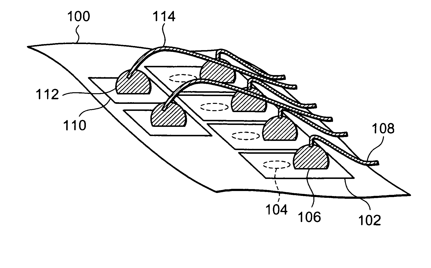
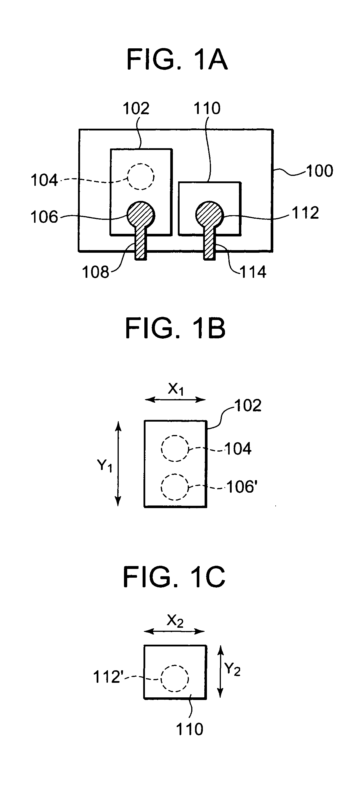
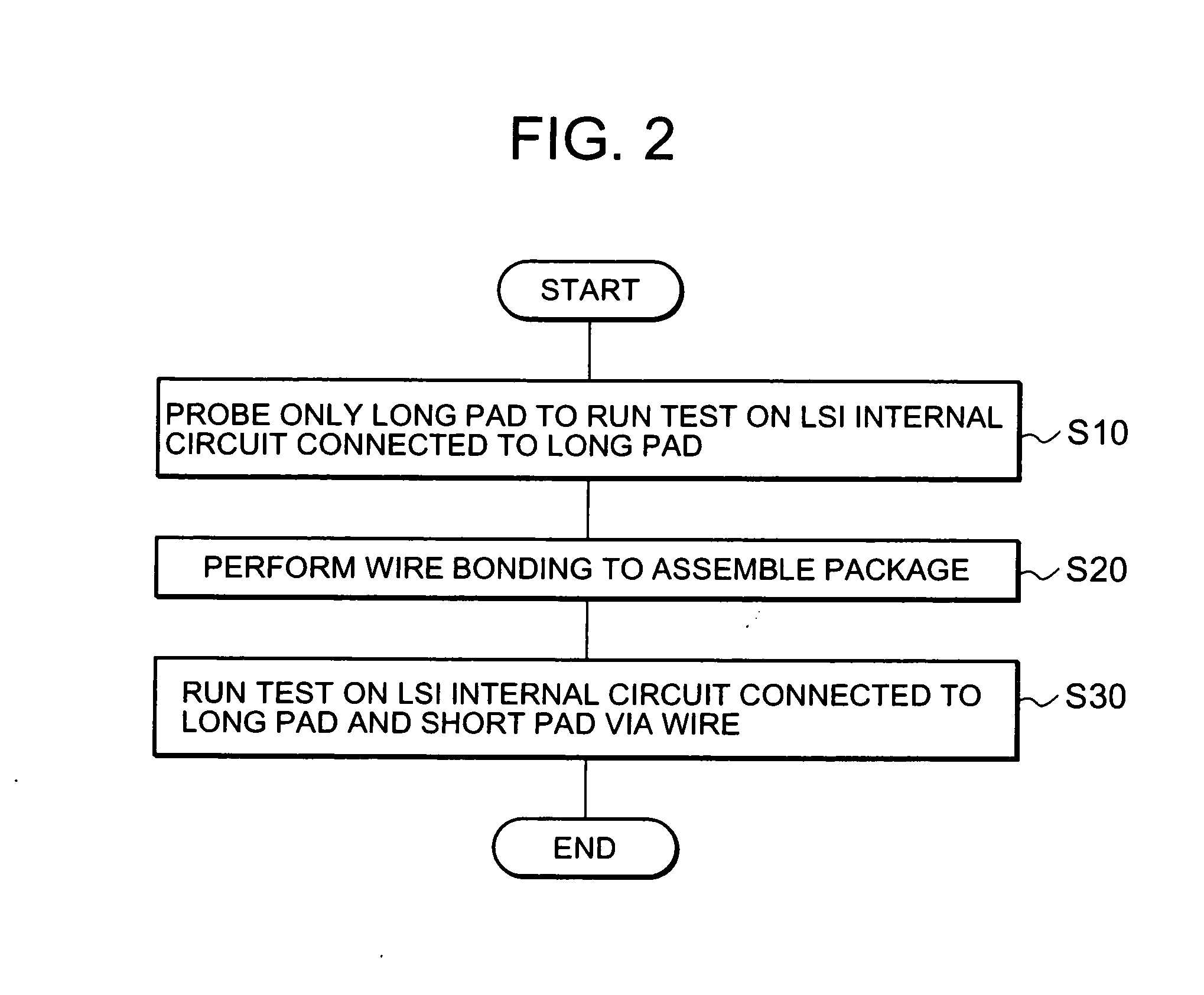
[0030]Hereinafter, an embodiment of the present invention is described with reference to the drawings. It should be noted that similar components are denoted by similar reference symbols in the respective drawings, and their descriptions are appropriately omitted.
[0031]In this embodiment, a semiconductor device includes a semiconductor chip region provided with a plurality of internal circuits, and a plurality of electrode pads which are provided in the vicinity of an outer edge of the semiconductor chip region and are each electrically connected to any one of the plurality of internal circuits. In other words, the semiconductor device is constructed in a chip form, and then the electrode pad is provided in the vicinity of the chip end of the semiconductor chip. The plurality of electrode pads each have a function of bonding a wire for supplying a signal or power sent from the outside to the internal circuits provided on the semiconductor chip. In this embodiment, the plurality of e...
PUM
 Abstract
Description
Claims
Application Information