

Method for improving ebg structures and multi-layer board applying the same
a multi-layer board and ebg technology, applied in the direction of cross-talk/noise/interference reduction, electrical apparatus construction details, conductive pattern formation, etc., can solve the problems of abnormal operation of electronic devices or circuits, abnormal operation of the whole system, and voltage variations at some positions, so as to prevent the generation of noise
- Summary
- Abstract
- Description
- Claims
- Application Information
AI Technical Summary
Benefits of technology
Problems solved by technology
Method used
Image

Examples
first embodiment
[0027]In the first embodiment of the present invention, according to the improved EBG structure, a bandgap from the low frequency to the high frequency is formed, so as to reduce the generation of the noises and provide a better power supply integrity for the digital signal system.
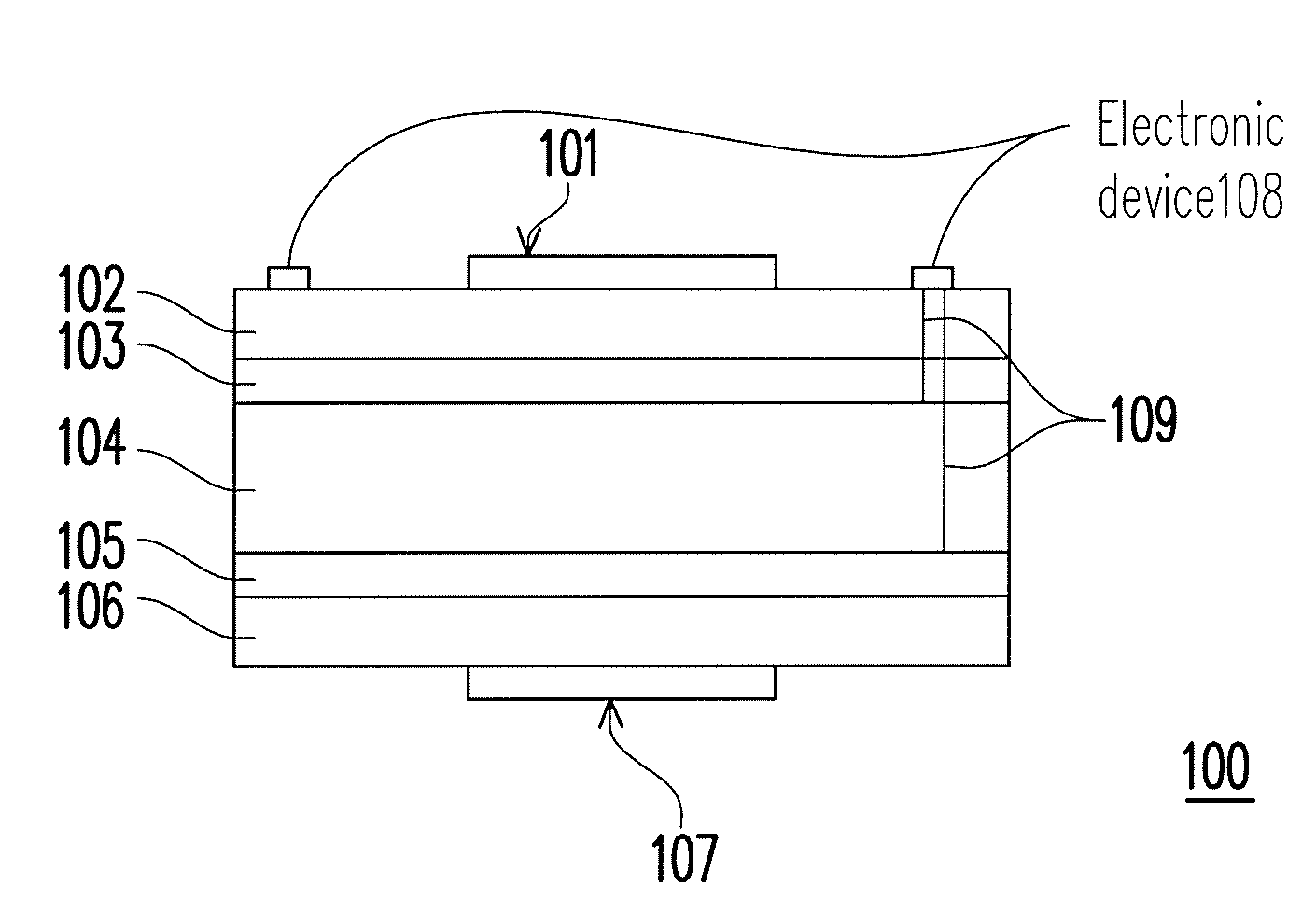
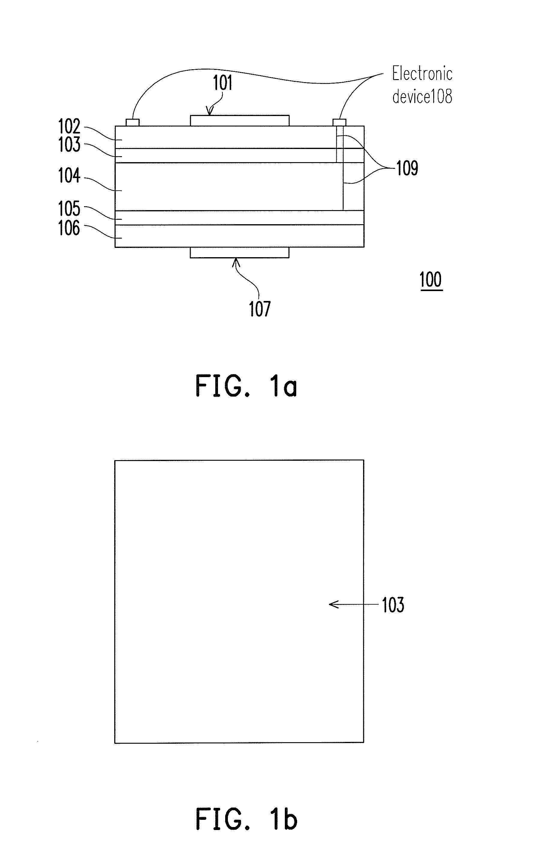
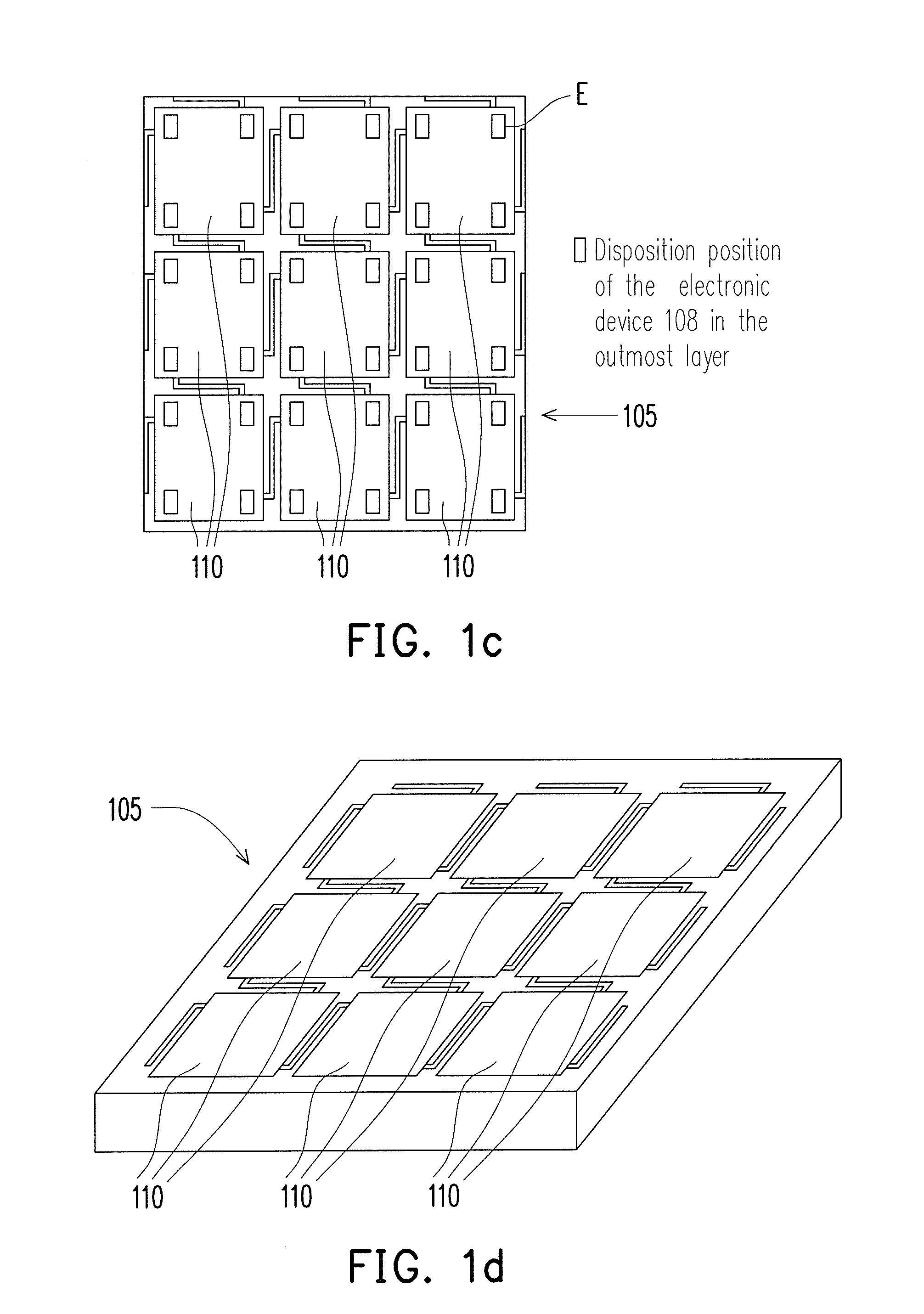
[0028]FIG. 1a is a cross-sectional view of a multi-layer board according to a first embodiment of the present invention. FIG. 1b is a schematic diagram of a ground layer of the multi-layer board. FIG. 1c is a schematic diagram of a power layer of the multi-layer board. FIG. 1d is a schematic diagram of a power layer having an EBG unit. FIG. 1e is a magnified diagram of the EBG unit.
[0029]Referring to FIG. 1a-FIG. 1e, as shown in FIG. 1a, the 4-layer board 100 at least includes signal layers 101 and 107, a ground layer 103, a power player 105 and dielectric layers 102, 104 and 106. Arrangement of the layers is just an example, which is not limited by the present invention. Such multi-layer board structure c...
second embodiment
[0055]FIG. 5 is a flowchart illustrating a method for improving an EBG structure according to a second embodiment of the present invention. Referring to FIG. 5, in step 501, a multi-layer board having at least one EBG unit is provided. Structures of the multi-layer board and the EBG unit are, for example, similar to that of the aforementioned embodiment, and therefore detailed description thereof will not be repeated herein.
[0056]Next, in step 502, a maximum input impedance of the EBG unit under a predetermined frequency band (for example, DC˜10 GHz) is measured, wherein a frequency corresponding to the maximum input impedance is regarded as the resonance frequency, and a capacitance is determined according to the measured resonance frequency. How to determine the capacitance according to the parallel resonance frequency is similar to that of the aforementioned embodiment, and therefore detailed description thereof will not be repeated herein.
[0057]In step 503, a minimum input imped...
PUM
| Property | Measurement | Unit |
|---|---|---|
| insertion loss | aaaaa | aaaaa |
| frequency | aaaaa | aaaaa |
| frequency | aaaaa | aaaaa |
Abstract
Description
Claims
Application Information