Sensor for a magnetic memory device and method of manufacturing the same

Inactive Publication Date: 2009-05-28
MICROMEM TECH
View PDF5 Cites 24 Cited by
  • Summary
  • Abstract
  • Description
  • Claims
  • Application Information

AI Technical Summary

Benefits of technology

[0010]The present invention encompasses a magnetic memory device that substantially obviates one or mo

Problems solved by technology

One serious limitation to this technology is related to tunneling that limits the erase / write cycle endurance and can induce catastrophic breakdown (after a maximum of about 106 cycles).
Moreover, the required charging time—which is of the order of 1 ms—is relatively long.
However, the need for an additional cycle to return a given bit to its original state for reading purposes (destructive read) aggravates the problems of dielectric fatigue.
This, in turn, is characterized by degradation in the ability to polarize the material.
Finally, fabrication process uniformity and control still remains a challenge.
The GMR structures showed a magnetoresistance of about 6%, but the exchange between the magnetic layers limited how quickly the magnetization could change direction.
Moreover magnetization curling from the edge of the strip imposed a limitation on the reduction in the cell size, or scaling.
PSV structures are amenable to scaling but the reported fields required to switch the hard magnetic layer are still too high for high density integrated circuits.
However, controlling the resistance uniformity (i.e., the tunneling barrier thickness and quality), and hence controlling the switching behavior from bit to bit remains a real challenge that has yet to be overcome in practical implementation.

Method used


Image

  • Sensor for a magnetic memory device and method of manufacturing the same
  • Sensor for a magnetic memory device and method of manufacturing the same
  • Sensor for a magnetic memory device and method of manufacturing the same

Examples


Embodiment Construction

General Description

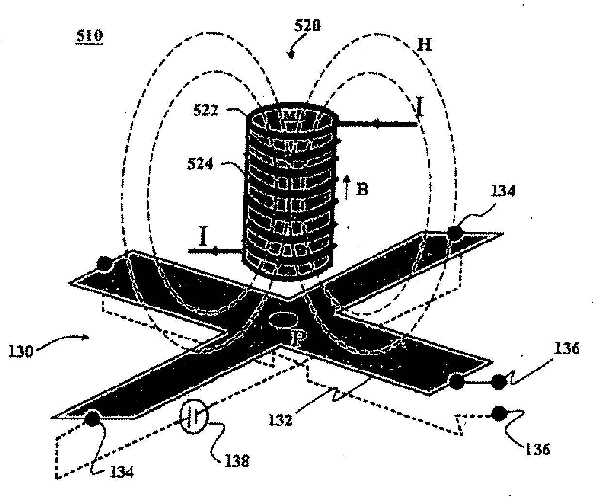
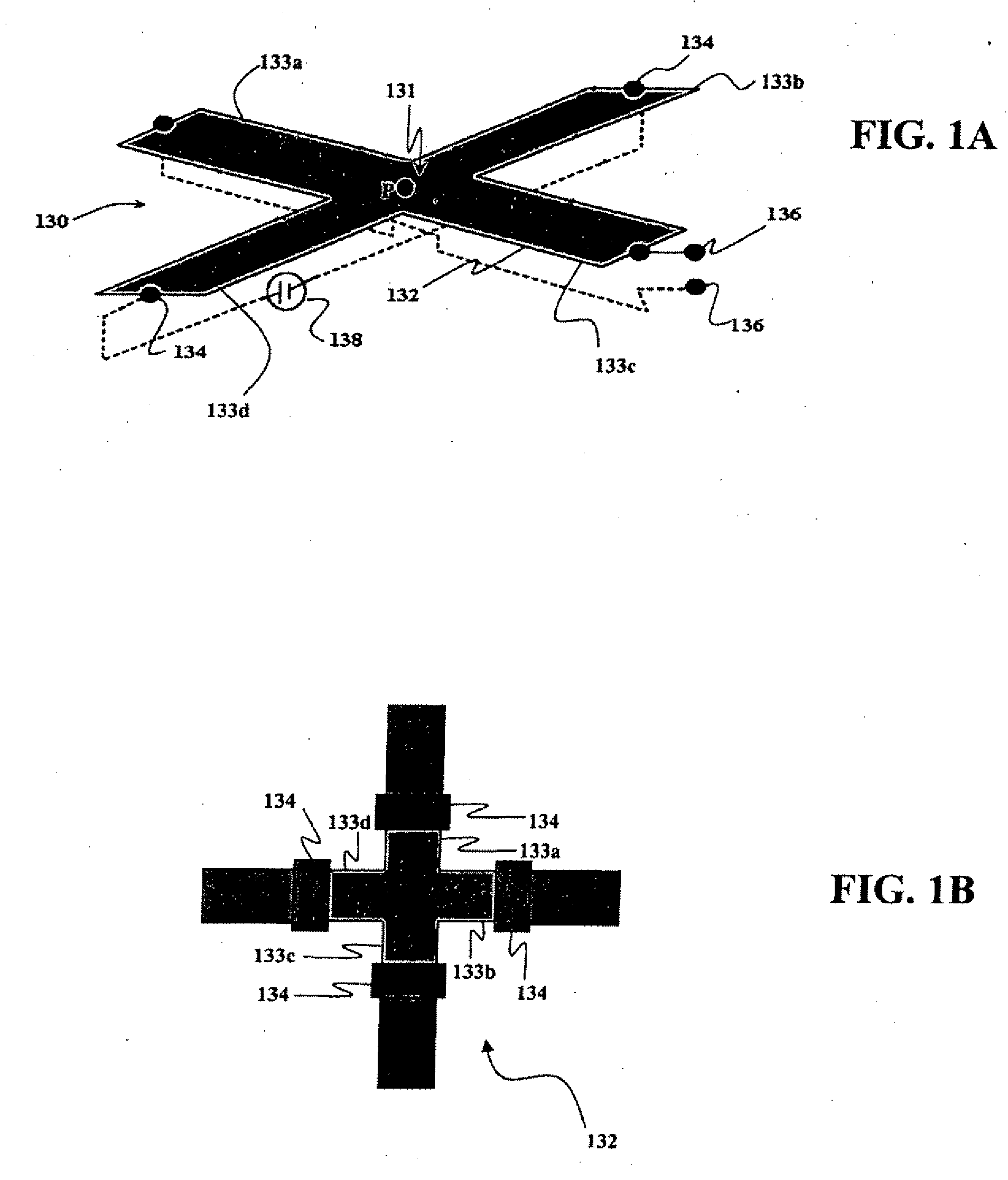
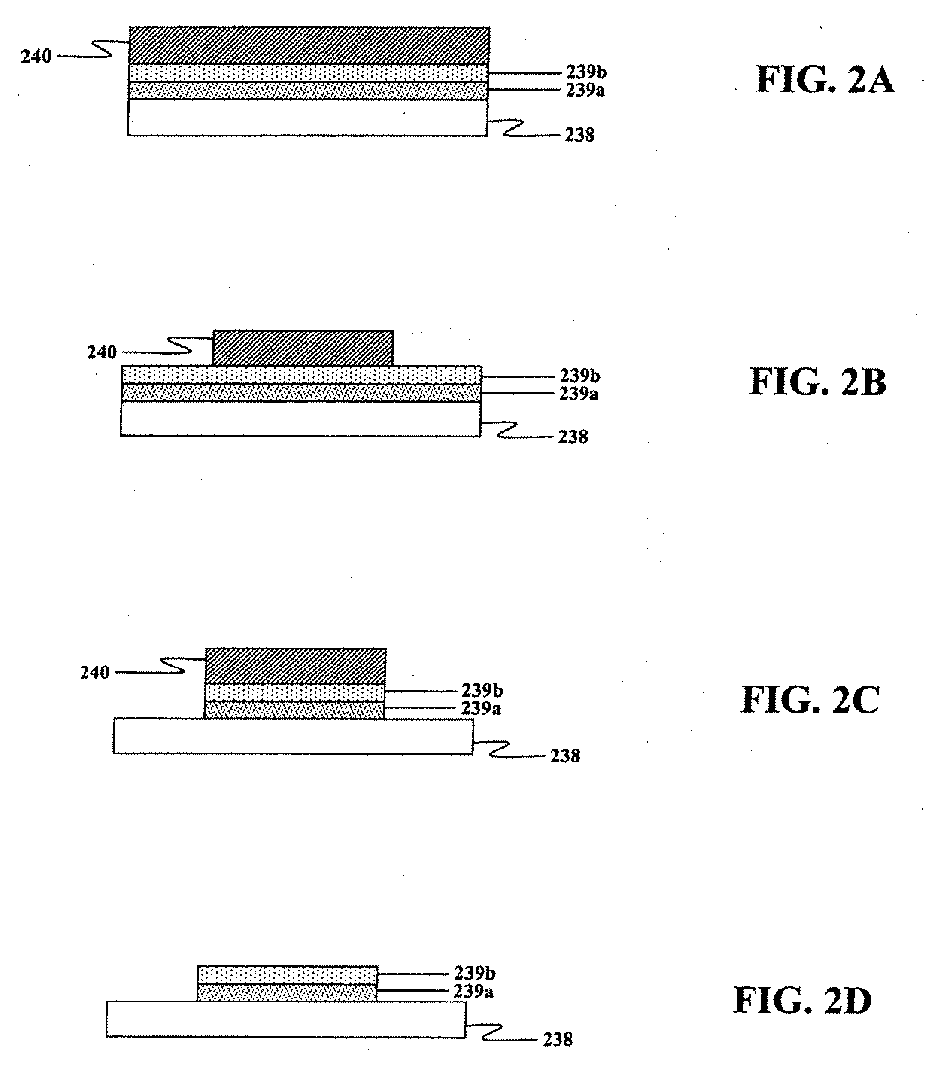
[0041]The invention encompasses methods for making a magnetic memory cell including a Hall effect sensor on a substrate including the steps of:[0042](i) preparing a substrate;[0043](ii) forming an amorphous layer on the substrate on the substrate;[0044](iii) heating the amorphous layer; and[0045](iv) epitaxially growing a material on the amorphous layer.

[0046]In one embodiment, the substrate is a silicon substrate.

[0047]In another embodiment, the amorphous layer is comprised of a group III-V material.

[0048]In another embodiment, the III-V material is a low temperature III-V material.

[0049]In another embodiment, the amorphous III-V material layer is GaAs.

[0050]In another embodiment, the epitaxially grown material is a 2DEG structure.

[0051]In another embodiment, the epitaxially grown material is a 2DEG structure constructed from AGaAs / GaAs.

[0052]In another embodiment, the method further includes using high electron mobility materials to form a Hall effect sensor on ...


PUM


Abstract

The invention encompasses fabrication methods including the steps of preparing a silicon substrate, forming an amorphous III-V material layer on the silicon substrate, heating the amorphous III-V material layer, and epitaxially growing III-V material on the amorphous III-V material layer.

Description

[0001]This application claims the benefit of pending U.S. provisional patent application No. 60 / 996,610, which was filed Nov. 27, 2007 and is incorporated herein by reference in its entirety.FIELD OF THE INVENTION[0002]The present invention encompasses memory devices and more particularly memory devices using magnetic memory elements.BACKGROUND OF THE INVENTION[0003]The rapid growth in the portable consumer product market (including the products for portable computing and communications) is driving the need for low power consumption non-volatile memory devices, with their inherent ability to retain stored information without power. The principal technology currently available in the marketplace for these applications is EEPROM (Electrically Erasable Programmable Read-Only Memory) technology, relying on charging (i.e., writing) or discharging (i.e., erasing) the floating-gate of a Metal-Oxide-Semiconductor (e.g., N-type) type transistor using so-called Fowler-Nordheim tunneling throu...

Claims


Application Information

Patent Timeline
IPC IPC(8): H01L21/00
CPCH01L43/14H01L27/222H10B61/00H10N52/01
Inventor IMAI, DARRENKUPER, CYNTHIA A.
Owner MICROMEM TECH
Why Eureka
Try Eureka