On-Die Terminators Formed of Coarse and Fine Resistors

a technology of resistors and on-die terminators, which is applied in the direction of logic circuits characterised by logic functions, pulse techniques, electronic switching, etc., can solve the problems of low current maximum per unit width that can be endured by polysilicon resistors, data signals are refractory, and it is difficult to form precise on-die terminators using n-wells. , to achieve the effect of less chip area, less n-wells, and less n-

Active Publication Date: 2009-06-04
TAIWAN SEMICON MFG CO LTD
View PDF27 Cites 4 Cited by
  • Summary
  • Abstract
  • Description
  • Claims
  • Application Information

AI Technical Summary

Benefits of technology

[0013]By forming on-die terminators using coarse and fine resistors, less chip area is used without sacrificing the accuracy of the resulting resistances. The embodiments of the present invention are also more scalable.

Problems solved by technology

When data signals are communicated between circuit devices, reflection of the data signals occurs if the impedances of devices mismatch.
However, the maximum currents per unit width that can be endured by polysilicon resistors are low, and hence polysilicon resistors typically occupy big chip areas.
It is thus difficult to form precise on-die terminators using n-wells.
Existing on-die terminators cannot satisfy both the requirements of reduced chip area usage and high accuracy at the same time.

Method used


Image

  • On-Die Terminators Formed of Coarse and Fine Resistors
  • On-Die Terminators Formed of Coarse and Fine Resistors
  • On-Die Terminators Formed of Coarse and Fine Resistors

Examples


Embodiment Construction

[0019]The making and using of the presently preferred embodiments are discussed in detail below. It should be appreciated, however, that the present invention provides many applicable inventive concepts that can be embodied in a wide variety of specific contexts. The specific embodiments discussed are merely illustrative of specific ways to make and use the invention, and do not limit the scope of the invention.

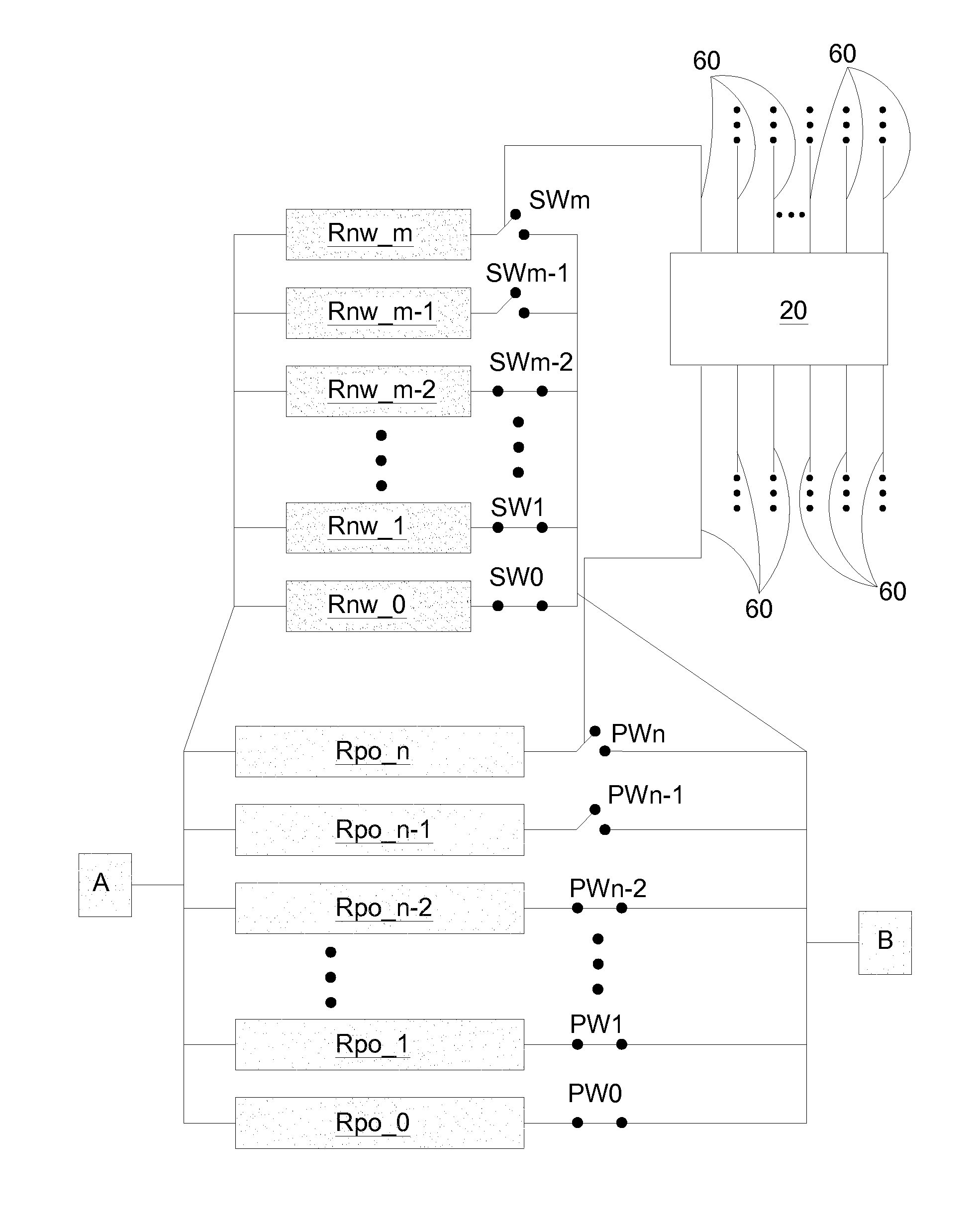
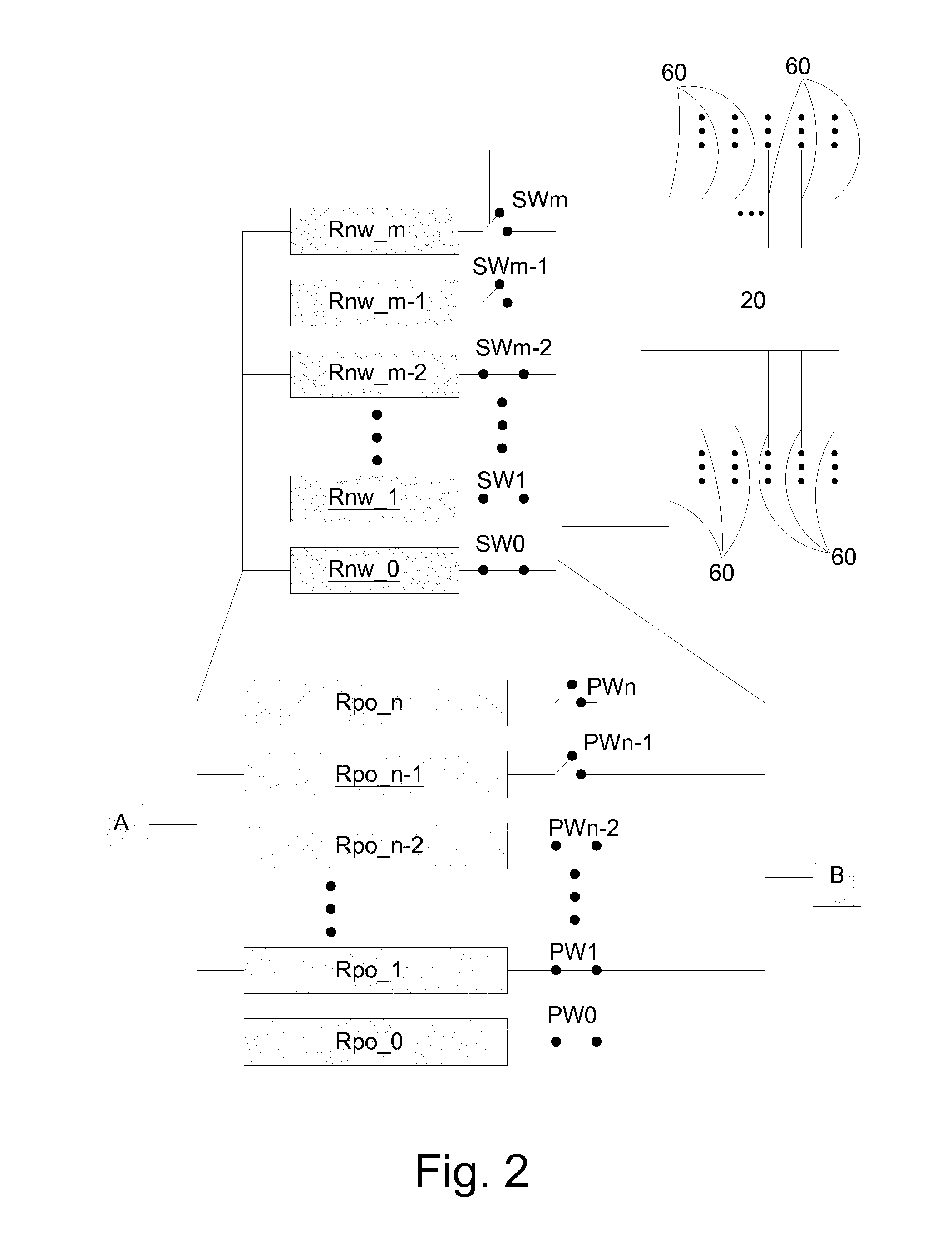
[0020]To terminate a transmission line, an on-die terminator may be fabricated to have a same resistance (or impedance) as the transmission line. However, due to process variations, it is difficult to fabricate an on-die terminator having a precise resistance. Further, when the on-die terminator is used, the temperature and the voltage applied on the on-die terminator also causes the change in the resistance of the on-die terminator. The resistance variations caused by process variations, temperature variations, and voltages (referred to as PVT variations) need to be compensa...


PUM


Abstract

An integrated circuit includes a semiconductor substrate; a first node; a second node; and a first plurality of resistors, each in a first plurality of resistor units. Each of the first plurality of resistor units includes a first end connected to the first node, and a second end connected to the second node. The integrated circuit further includes a second plurality of resistors, each in a second plurality of resistor units. Each of the second plurality of resistor units includes a first end connected to the first node, and a second end connected to the second node. The first plurality of resistors is formed of a first material. The second plurality of resistors is formed of a second material different from the first material. The integrated circuit further includes a switch in one of the first and the second plurality of resistor units and serially connected to a resistor.

Description

TECHNICAL FIELD[0001]This invention relates generally to semiconductor devices, and more particularly to on-die terminators for signal transmissions.BACKGROUND[0002]When data signals are communicated between circuit devices, reflection of the data signals occurs if the impedances of devices mismatch. Thus, an information signal exchange system requires a terminal resistor that terminates a signal transmission line, and the terminal resistor need to have an impedance matching the impedance of the signal transmission line. The terminal resistor suppresses the reflection of a received signal to raise the integrity of the transferred signals.[0003]The terminal resistor may be located on the inside or outside of a semiconductor chip, which typically has integrated circuits for processing the data signals. The terminal resistor in a semiconductor chip is usually called an on-chip terminator, on-die terminator, or active terminator.[0004]To be effectively used in a semiconductor chip, the ...

Claims


Application Information

Patent Timeline
Patent Type & Authority Applications(United States)
IPC IPC(8): H03K17/16
CPCH01L28/20H01L27/0802
Inventor CHEN, CHUNG-HUI
Owner TAIWAN SEMICON MFG CO LTD
Why Eureka
Try Eureka