Display device and driving method thereof

Active Publication Date: 2009-06-04
SEMICON ENERGY LAB CO LTD
View PDF17 Cites 48 Cited by
  • Summary
  • Abstract
  • Description
  • Claims
  • Application Information

AI Technical Summary

Benefits of technology

[0039]As for a liquid crystal display device and a driving method thereof according to the present invention, even when one pixel is divided into a plurality of sub-pixels in order to improve viewing angle and when a method for improving viewing angle in which different signal voltages are applied to sub-pixel is employed, increase in the circuit scale, increase in driving speed of a circuit, or the like for driving sub-pixels does not occur. As the result, reduction in power consumption and in manufacturing cost can be realized. Moreover, an accurate signal can be input to each sub-pixel, so that quality of still image display can be improved. Furthermore,

Problems solved by technology

Moreover, signal line drivers (also referred to as a data driver or a source driver) for driving each signal line are also necessary, so that there is a problem that the manufacturing cost and power consumption increase by increasing circuit scale.
Thus, there is a problem that the method is disadvantageous

Method used


Image

  • Display device and driving method thereof
  • Display device and driving method thereof
  • Display device and driving method thereof

Examples


embodiment mode 1

[0062]First, an operation in which a pixel circuit should have in order to solve the above objects and examples of a pixel structure which realize thereof is described. The operation in which a pixel circuit should have in order to solve the above objects mainly includes following two operations. That is, (operation A) different voltages are written to the plurality of sub-pixels included in a pixel by one time of writing, and (operation B) a period in which all sub-pixels display black color is provided in one frame period. With realization of operation A, viewing angle can be improved without increasing circuit scale, driving speed, or the like for driving sub-pixels. In addition, operation B is realized while operation A is realized, so that viewing angle is improved, power consumption is reduced, and image quality of moving image display is improved. As thus described, not only improvement of one characteristic among characteristics which a liquid crystal display device has, but...

embodiment mode 2

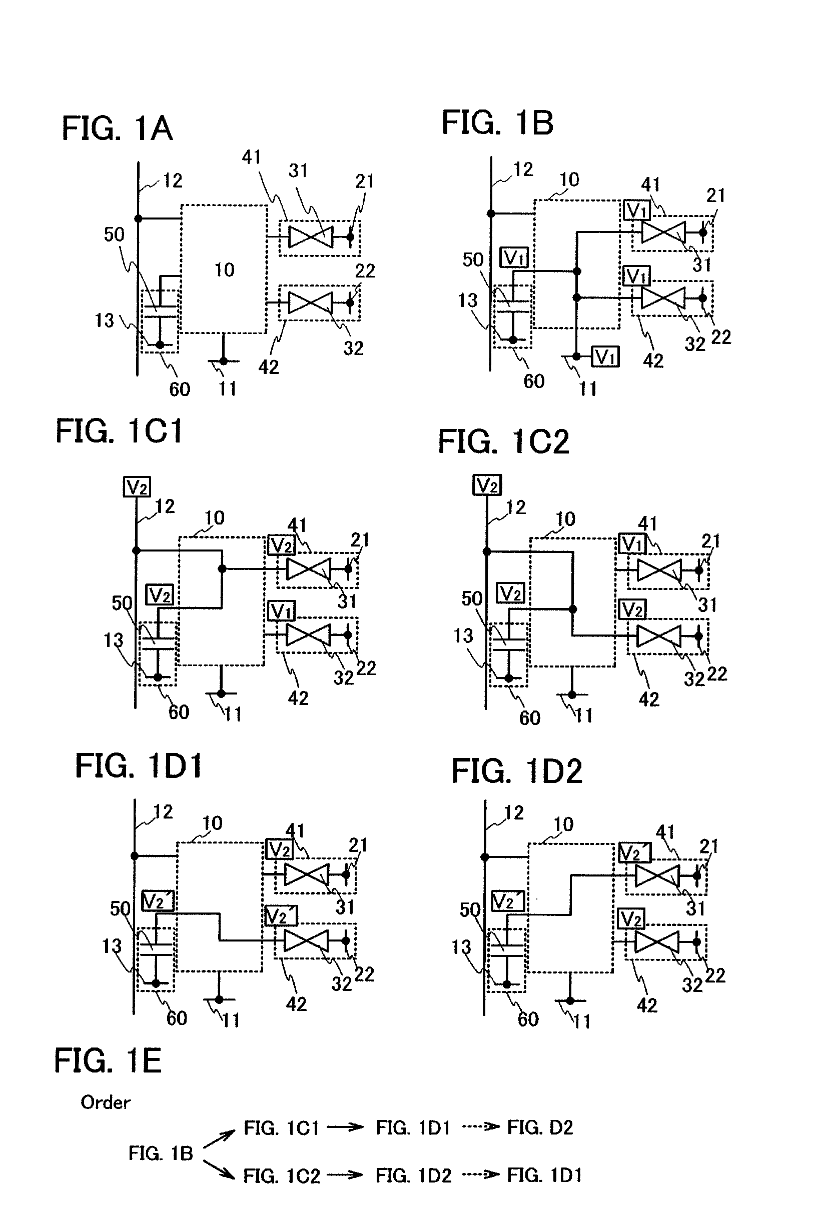
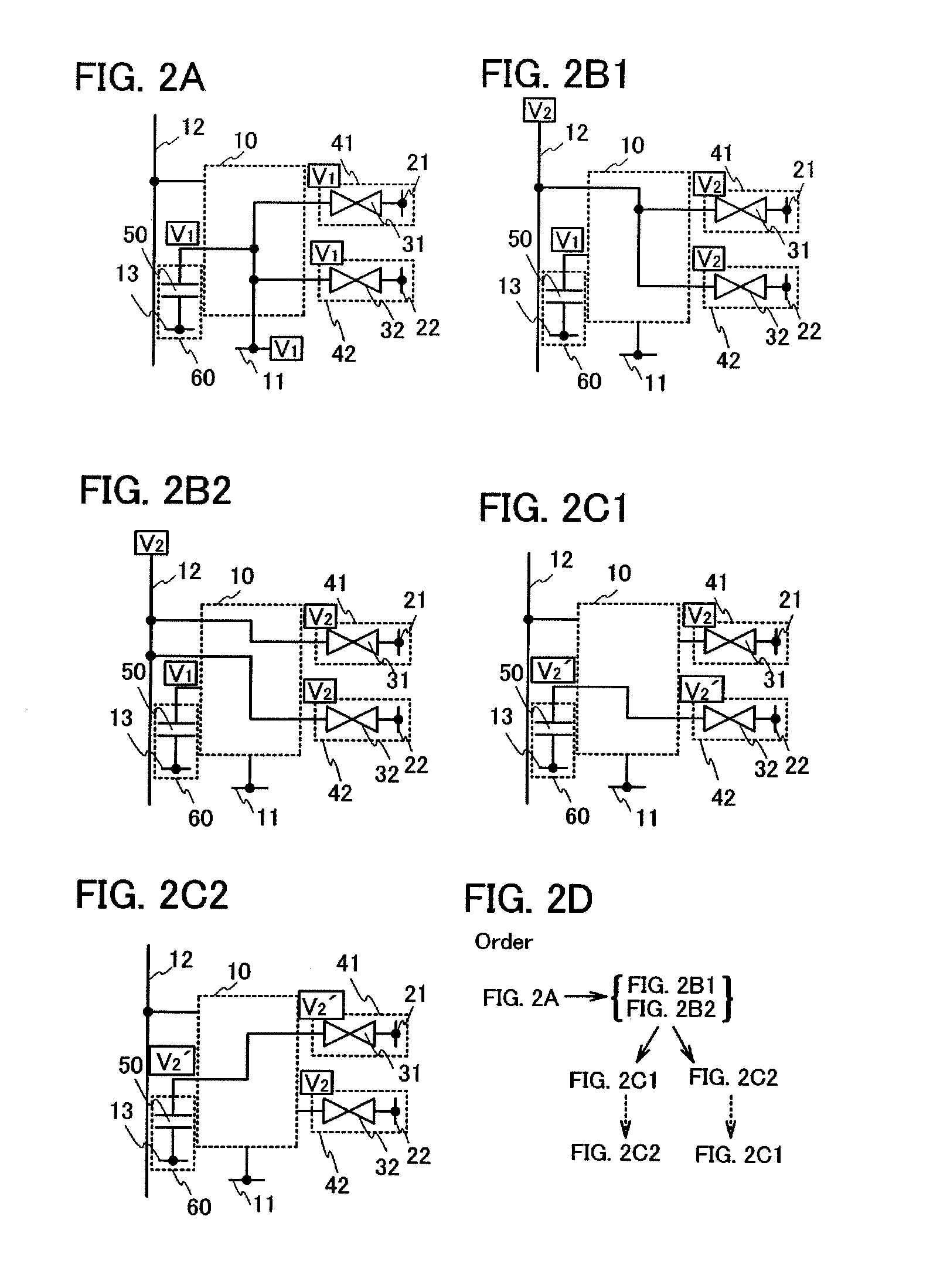
[0125]In this embodiment mode, the first pixel structure described in Embodiment Mode 1 is specifically described. In Embodiment Mode 1, description is made only focused on the conducting state inside of the first circuit 10. In this embodiment mode, description is made about the conducting states of a plurality of switches included in the first circuit 10, and about the timing (a timing chart) of switching the conducting states of each switch.

[0126]As a circuit example (1), FIGS. 6A to 6D illustrate a circuit which can realize function (1) and a part of the function (3) of the first circuit 10 described in Embodiment Mode 1. Here, the part of the function (3) is the function including a conducting state in which the data voltage is selectively written only in the first capacitor element 50 out of the function (3) which is already described.

[0127]First, a circuit example illustrated in FIG. 6A is described. The circuit example illustrated in FIG. 6A includes a first switch (SW1), a ...

embodiment mode 3

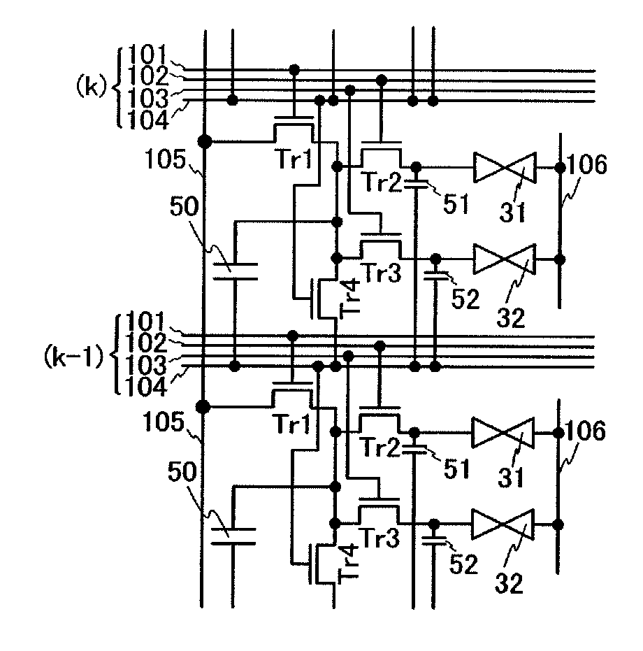
[0207]In this embodiment mode, various circuit examples described in Embodiment Mode 2 are specifically described. In Embodiment Mode 2, conducting states and timing charts of the plurality of switches included in the first circuit 10 are described. In this embodiment mode, as switches shown in the various circuit examples described in Embodiment Mode 2, the case of using the transistors is described in detail with reference to specific examples of circuit diagrams.

[0208]First, a specific example of the circuit example (1) in Embodiment Mode 2 is described. A circuit illustrated in FIG. 11A is a specific example (1) of the circuit example (1) illustrated in FIG. 6A and includes a first transistor Tr1, a second transistor Tr2, a third transistor Tr3, a fourth transistor Tr4, the first capacitor element 50, the second capacitor element 51, the third capacitor element 52, the first liquid crystal element 31, the second liquid crystal element 32, a first wiring 101, a second wiring 102,...


PUM


Abstract

With a display device using a pixel which includes a sub-pixel, the display device with improved viewing angle and quality of moving image display is provided without increase in power consumption by driving of the sub-pixel. A circuit which can change conducting states by a plurality of switches is provided, and charge in a plurality of sub-pixels and a capacitor element is transported mutually, so that desired voltage is applied to the plurality of sub-pixels without applying voltage in plural times from external. Moreover, a period in which each sub-pixel displays black is provided in accordance with transfer of charge.

Description

TECHNICAL FIELD[0001]The present invention relates to a display device and a semiconductor device. The present invention relates to an electronic device having the display device in a display portion.BACKGROUND ART[0002]A liquid crystal display device has some advantages such as thin, light weight, low power consumption, or the like, compared to a display device using a cathode-ray tube. Further, since a liquid crystal display device can be widely applied to from the small-sized display device having a few inches of diagonal of a display portion to the large-sized display device having more than 100 inches, the liquid crystal display device is widely used as a display device of various electronic devices such as a mobile phone, a still camera, a video camera, a television receiver, and the like.[0003]While the liquid crystal display device has excellent general versatility, there is a problem in that image quality is low compared to other display devices such as CRT and the like. Th...

Claims


Application Information

Patent Timeline
IPC IPC(8): G02F1/1343G02F1/1345
CPCG09G3/207G09G3/3607G09G3/3233G09G2300/0443G09G2300/0447G09G3/3648G02F1/133G02F1/1368G09G3/36
Inventor YOSHIDA, YASUNORI
Owner SEMICON ENERGY LAB CO LTD
Why Eureka
Try Eureka