Line edge roughness reduction and double patterning

a technology of double patterning and line edge roughness, which is applied in the direction of photomechanical treatment, instruments, electrical equipment, etc., can solve the problems of degrading device performance, short and/or open circuits, and interconnect lines suffering from line edge roughness (ler), so as to reduce the effect of reducing the size of the trenches

Inactive Publication Date: 2009-06-04
APPLIED MATERIALS INC
View PDF10 Cites 27 Cited by
  • Summary
  • Abstract
  • Description
  • Claims
  • Application Information

AI Technical Summary

Benefits of technology

[0008]Embodiments may provide a double exposure lithographic method comprising: depositing a first layer of photoresist over a hard mask layer over a bottom layer on a substrate; exposing the first photoresist layer with a first pattern; performing a first post-exposure bake and first develop of the exposed first photoresist layer to form a first patterned photoresist layer; applying a first shrink coating over the first patterned photoresist; baking the first shrink coating and first patterned photoresist, wherein the first shrink coating contracts, pulling the photoresist into the trenches of the first patterned photoresist, thus reducing the sizes of the trenches patterned in the first patterned photoresist; rinsing the first shrink coating from the first patterned photoresist; performing a first post develop bake of the first patterned layer of photoresist; transferring the first pattern into the hard mask layer, to form a first patterned hard mask layer; removing the first patterned photoresist; depositing a second layer of photoresist over the first patterned hard mask layer; exposing the second photoresist layer with a second pattern; performing a second post-exposure bake of the second photoresist layer; develo...

Problems solved by technology

Furthermore, as lithographic processes are pushed to the limit, interconnect lines suffer from line edge roughness (LER).
Interconnect lines having a high LER may result in...

Method used


Image

  • Line edge roughness reduction and double patterning
  • Line edge roughness reduction and double patterning
  • Line edge roughness reduction and double patterning

Examples


Embodiment Construction

[0015]In the following description, various aspects of the present invention will be described, and various details set forth in order to provide a thorough understanding of the present invention. However, it would be apparent to those skilled in the art that the present invention may be practiced with only some or all of the aspects of the present invention, and the present invention may be practiced without the specific details. In other instances, well-known features are admitted or simplified in order not to obscure the present invention.

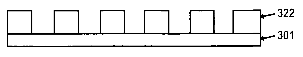
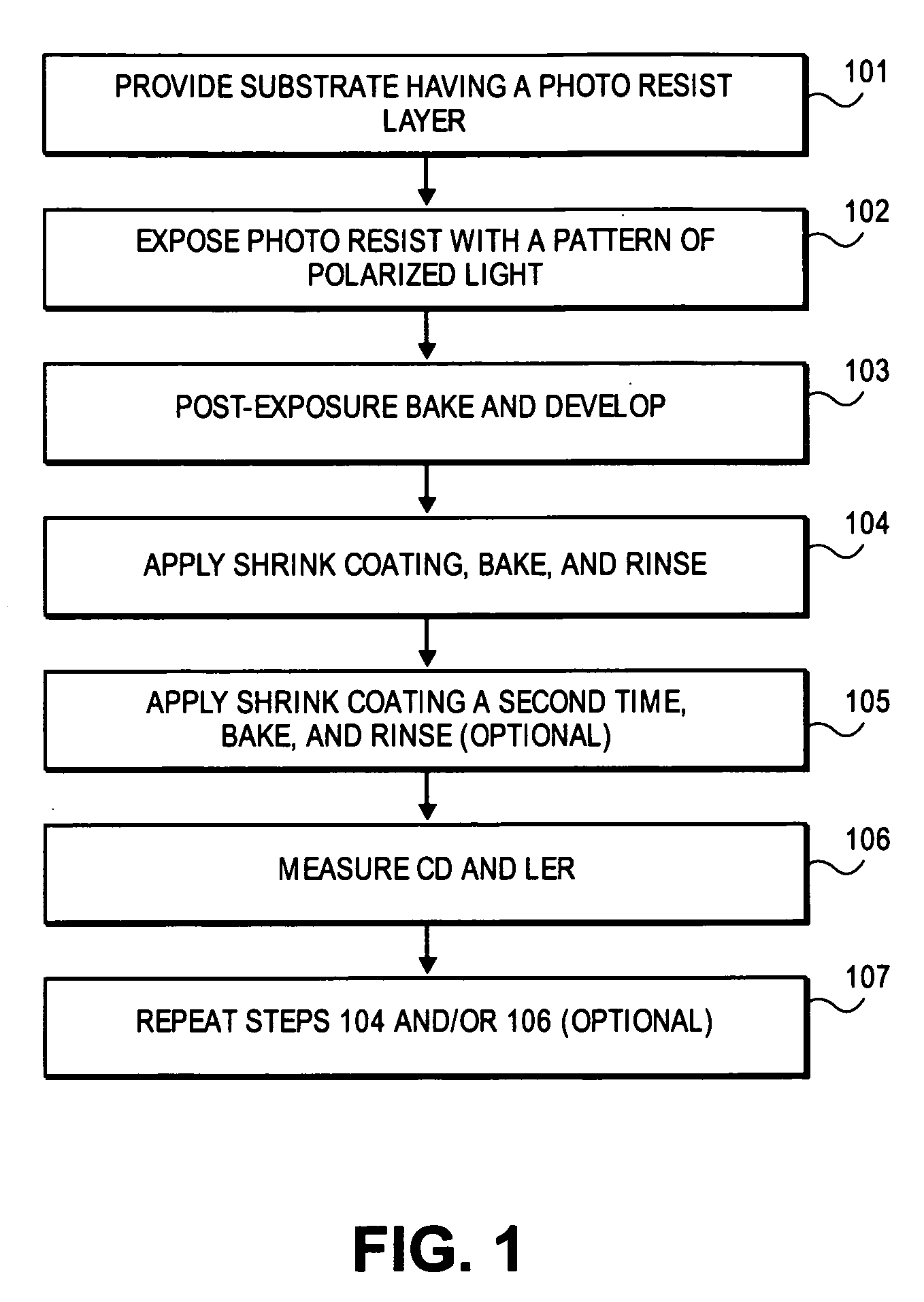
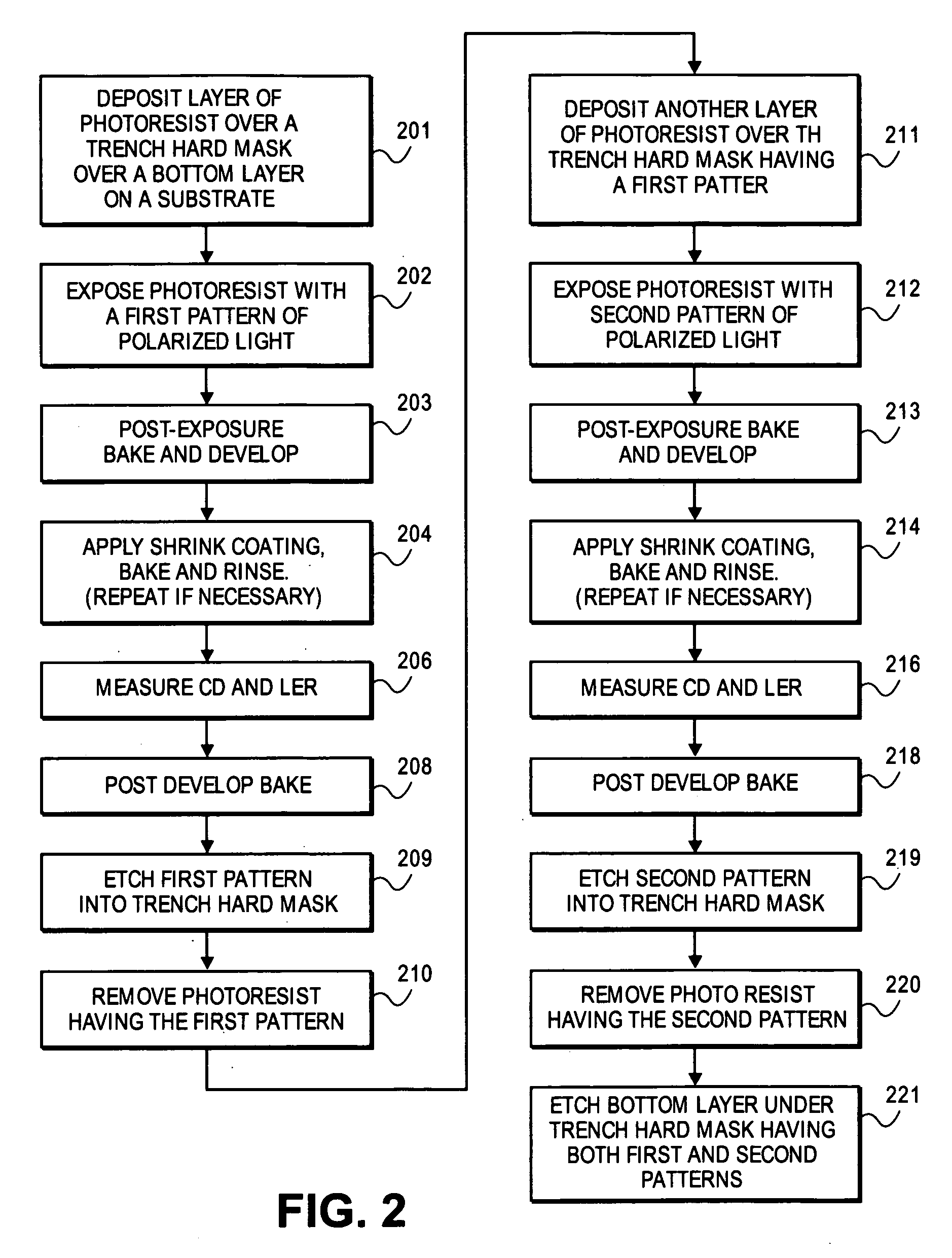
[0016]It should be understood that FIGS. 1 through 4B are merely illustrative and may not be drawn to scale. While certain exemplary embodiments have been described and shown in the accompanying drawings, it is to be understood that such embodiments are merely illustrative and not restrictive of the current invention, and that this invention is not restricted to the specific constructions and arrangements shown and described since modifications ...


PUM


Abstract

Embodiments of the present invention relate to lithographic processes used in integrated circuit fabrication for improving line edge roughness (LER) and reduced critical dimensions (CD) for lines and/or trenches. Embodiments use the combinations of polarized light lithography, shrink coating processes, and double exposure processes to produce synergetic effects in the formation of trench structures having good resolution, reduced CDs, reduced pitch, and reduced LER in the lines and/or trenches of the patterned interconnect structures.

Description

[0001]This application claims the benefit of U.S. Provisional Application No. 60 / 933,270, filed Jun. 4, 2007, the entire contents of which are hereby incorporated by reference herein.BACKGROUND OF THE INVENTION[0002]1. Field of the Invention[0003]The present invention relates to the field of integrated circuit fabrication. Particularly in lithographic processes for improving line edge roughness (LER) and reduced critical dimensions (CD) for lines and trenches.[0004]2. Discussion of Related Art[0005]The semiconductor industry is continually pursuing smaller and smaller geometries of the structures used in semiconductor devices. As the device geometries become smaller, more devices are fabricated into the same area of semiconductor substrate. Therefore, the number of interconnect lines in the same area of substrate must also increase, thus requiring that the sizes of the interconnect lines and the spacing between the interconnect lines also decrease in size. This results in the need t...

Claims


Application Information

Patent Timeline
IPC IPC(8): H01L21/311
CPCG03F7/2006G03F7/40H01L21/31144H01L21/0337H01L21/0338H01L21/0273
Inventor DAI, HUIXIONGXU, XUMOUNGAI, CHRISTOPHER S.
Owner APPLIED MATERIALS INC
Why Eureka
Try Eureka