Manufacturing apparatus for semiconductor device and manufacturing method for semiconductor device

a manufacturing method and technology for semiconductor devices, applied in the direction of coatings, basic electric elements, chemical vapor deposition coatings, etc., can solve the problems of reducing the uniformity of film thickness and difficulty in achieving high productivity, and achieve the effect of high productivity

Active Publication Date: 2009-06-04
NUFLARE TECH INC
View PDF12 Cites 196 Cited by
  • Summary
  • Abstract
  • Description
  • Claims
  • Application Information

AI Technical Summary

Benefits of technology

[0012]It is therefore an object of the present invention to provide a manufacturing apparatus for a semiconductor device and a manufacturing method for a semiconductor devi

Problems solved by technology

As described above, for example, in a thick film formation process for a semiconductor device, there are some problems, such as difficulty in ac

Method used


Image

  • Manufacturing apparatus for semiconductor device and manufacturing method for semiconductor device
  • Manufacturing apparatus for semiconductor device and manufacturing method for semiconductor device
  • Manufacturing apparatus for semiconductor device and manufacturing method for semiconductor device

Examples


first embodiment

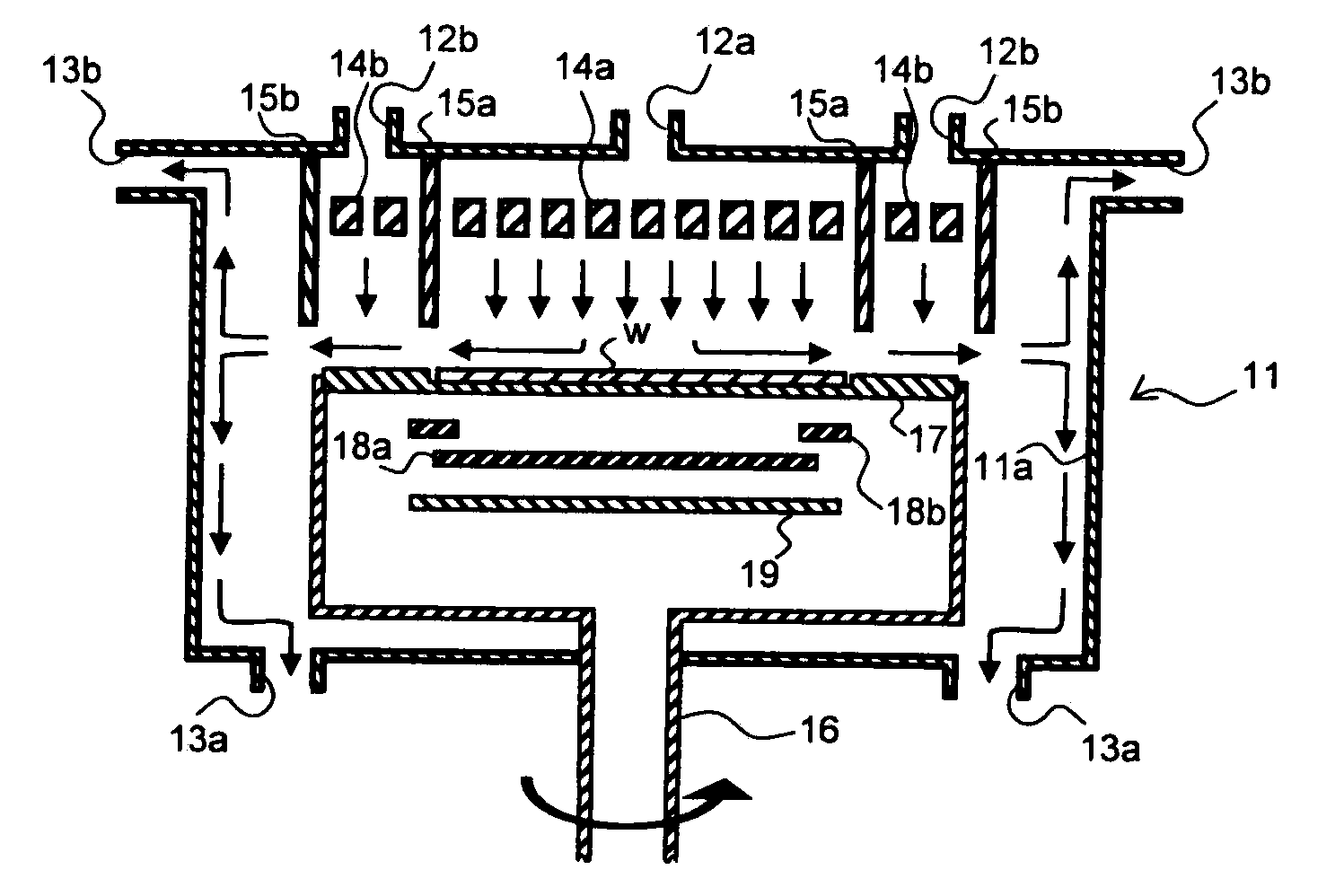
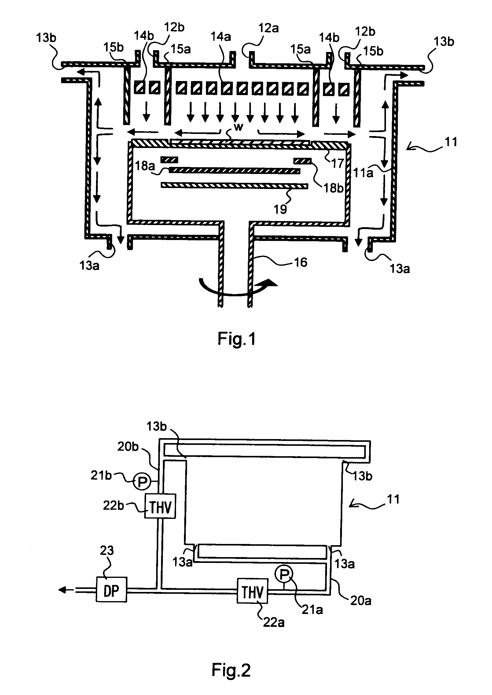
[0027]FIG. 1 is a sectional view of a manufacturing apparatus for a semiconductor device according to the present embodiment. In a reaction chamber 11 in which film formation for a wafer w is performed, gas supply ports 12a and 12b are provided. The gas supply ports 12a and 12b are connected to a gas supply unit (not shown) for supplying process gas including source gas, such as TCS and dichlorosilane, onto the wafer w from an upper portion of the reaction chamber 11 and a gas supply port 12b connected with a gas supply unit (not shown) for supplying dilution gas, film formation reaction suppression gas or cleaning gas onto the outer periphery of the wafer, respectively.

[0028]On upper portions of side walls and a bottom wall of the reaction chamber 11, plural, for example, two gas exhaust ports 13a and plural, for example, two gas exhaust ports 13b are provided, respectively. The gas exhaust ports 13a, 13b are connected with a gas exhaust unit for exhausting gas and controlling the ...

second embodiment

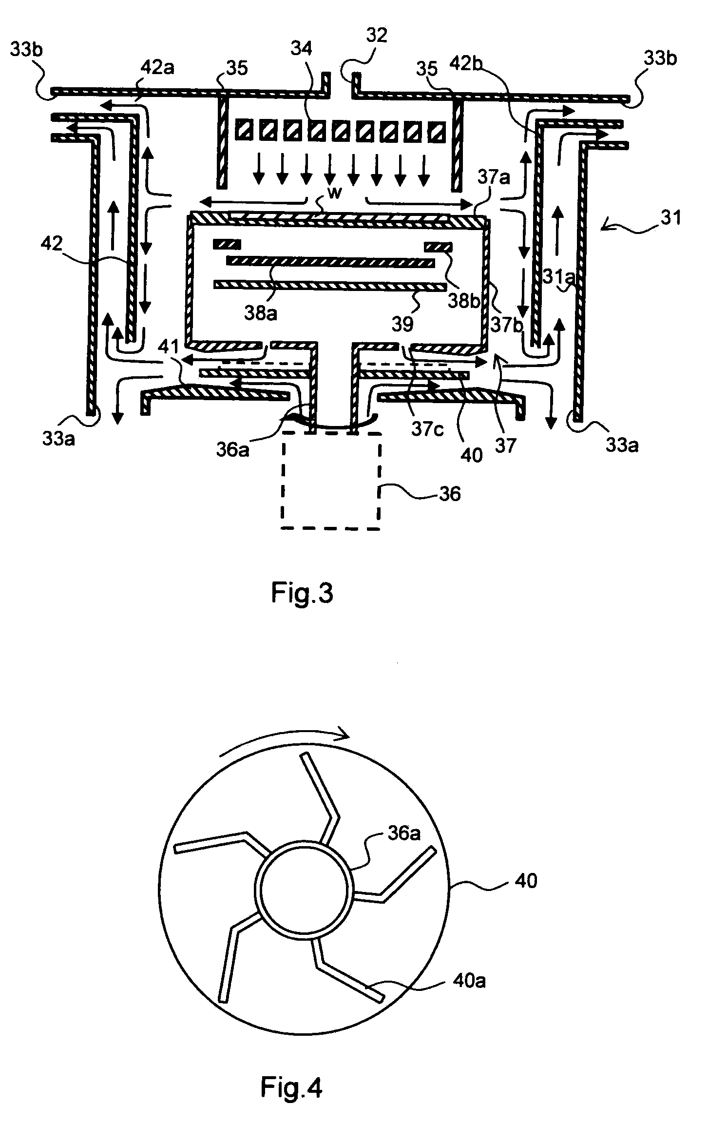
[0051]FIG. 3 is a sectional view of a manufacturing apparatus for a semiconductor device according to the present embodiment. In a reaction chamber 31 in which film formation for a wafer w is performed, a gas supply port 32 is provided. The gas supply port 32 is connected to a gas supply unit (not shown) for supplying process gas including source gas, such as TCS and dichlorosilane onto the wafer w from an upper portion of the reaction chamber 31. A bottom of the reaction chamber 31, plural, for example, two gas exhaust ports 33a are provided, and on upper portion of side wall of the reaction chamber 31, plural, for example, two gas exhaust ports 33b are provided, respectively in the same as for First Embodiment. The gas exhaust ports 33a, 33b are are provided for exhausting gas and controlling the pressure in the reaction chamber 31 to be constant (atmospheric-pressure).

[0052]On the upper portion of the reaction chamber 31, there is provided rectifying plate 34 for supplying proces...


PUM

PropertyMeasurementUnit
Pressureaaaaaaaaaa
Distanceaaaaaaaaaa

Abstract

A manufacturing apparatus for a semiconductor device, includes: a reaction chamber to which a wafer w is loaded; a gas supply port for supplying first process gas including source gas from an upper portion of the reaction chamber; a first rectifying plate for supplying the first process gas onto the wafer in a rectifying state; a first gas exhaust port for exhausting gas from a lower portion of the reaction chamber; a second gas exhaust port for exhausting gas from the upper portion of the reaction chamber; a heater for heating the wafer w; a susceptor for retaining the wafer w; and a rotation drive unit for rotating the wafer w.

Description

CROSS-REFERENCE TO RELATED APPLICATIONS[0001]This application is based upon and claims the benefit of priority from the prior Japanese Patent Applications No. No. 2007-308852 filed on Nov. 29, 2007, No. 2008-075957 filed on Mar. 24, 2008, the entire contents of which are introduced herein by reference.BACKGROUND OF THE INVENTION[0002]1. Field of the Invention[0003]The present invention relates to a manufacturing apparatus for a semiconductor device and a manufacturing method for a semiconductor device, which are used for a film formation on a semiconductor wafer by supplying process gas while heating the wafer.[0004]2. Description of the Related Art[0005]In recent years, with demands of further price reduction and high performance of a semiconductor device, there has been required high productivity in a film formation process as well as high quality of the semiconductor device such as improvement in uniformity of a film thickness.[0006]To satisfy such requirements, there has been us...

Claims


Application Information

Patent Timeline
IPC IPC(8): H01L21/302B05B3/02
CPCH01L21/02381H01L21/0262H01L21/68792H01L21/67109H01L21/68785H01L21/67017
Inventor YAJIMA, MASAYOSHISUZUKI, KUNIHIKO
Owner NUFLARE TECH INC
Why Eureka
Try Eureka