

Package substrate having electrically connecting structure
- Summary
- Abstract
- Description
- Claims
- Application Information
AI Technical Summary
Benefits of technology
Problems solved by technology
Method used
Image

Examples
Embodiment Construction
[0023]The present invention is herein illustrated with specific embodiments, so that one skilled in the pertinent art can easily understand other advantages and effects of the present invention from the disclosure of the invention.
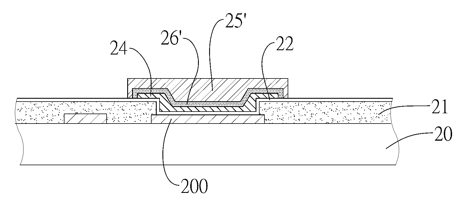
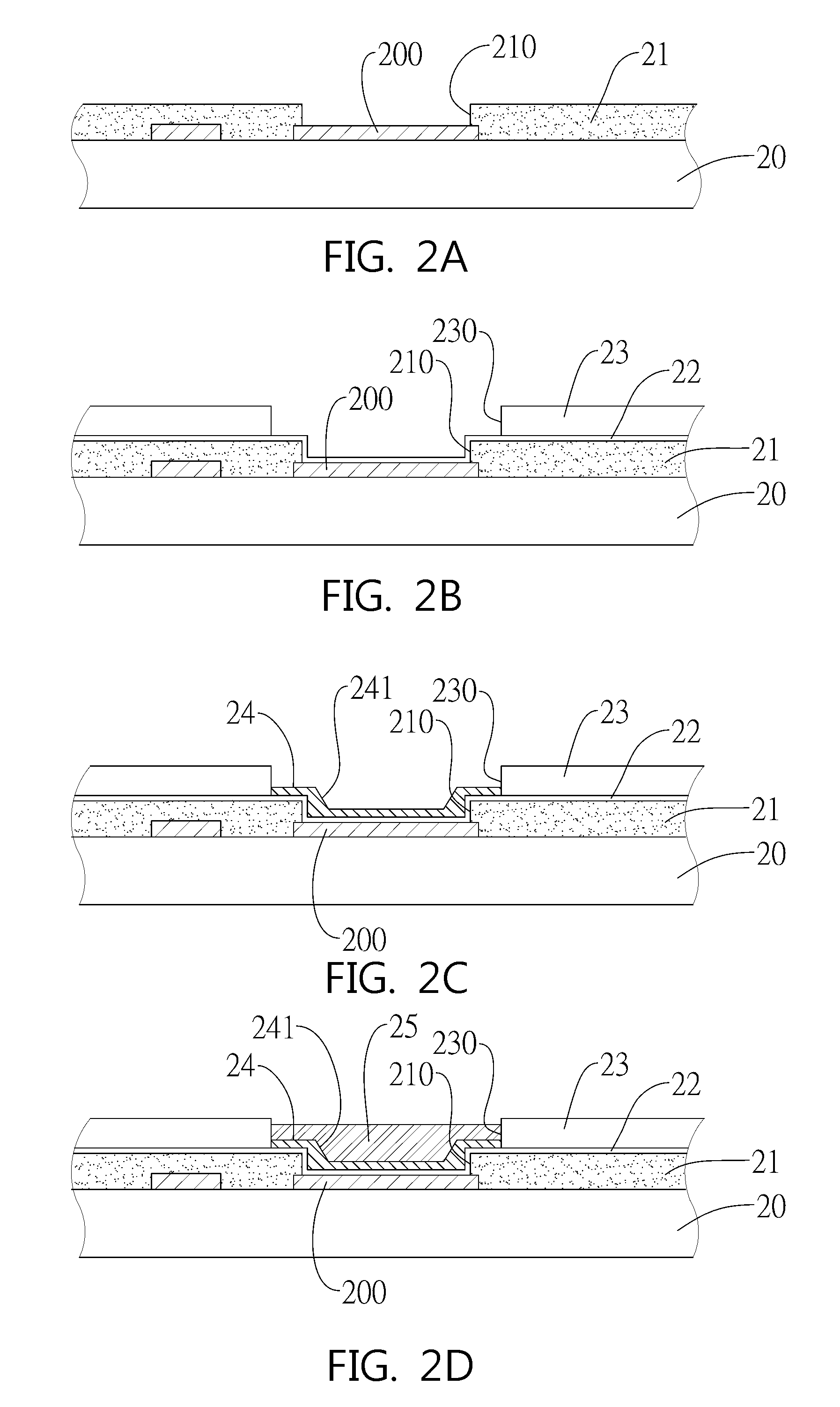
[0024]FIGS. 2A to 2E are cross-sectional views showing a method of fabricating a package substrate having an electrically connecting structure according to the present invention.
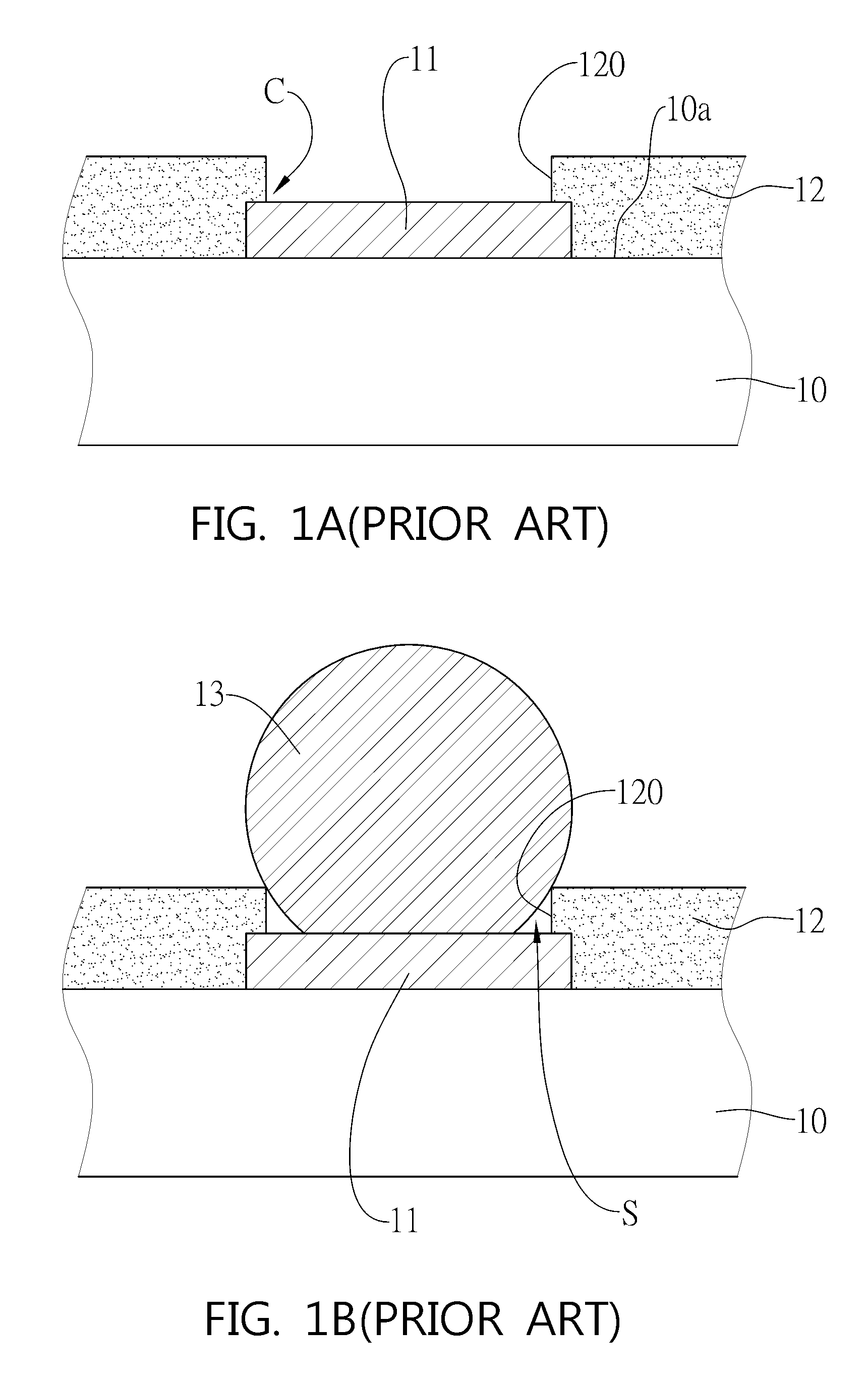
[0025]Referring to FIG. 2A, a package substrate substance 20 with at least a surface having a plurality of electrically connecting pads 200 formed thereon is provided. The package substrate substance 20 is bi-layered or tri-layered and has a finalized circuit layout. The electrically connecting pads 200 are electrically connected to an inner-layer circuit via a conductive blind via (not shown).
[0026]An insulating protective layer 21 is formed on the package substrate substance 20, by coating the package substrate substance 20 with the insulating protective layer 21 by stencil print...
PUM
 Abstract
Description
Claims
Application Information