Liquid crystal display device and fabricating method thereof

a technology of liquid crystal display and fabrication method, which is applied in the direction of printed circuits, instruments, optics, etc., can solve problems such as defective lcds

Active Publication Date: 2009-06-11
LG DISPLAY CO LTD
View PDF4 Cites 31 Cited by
  • Summary
  • Abstract
  • Description
  • Claims
  • Application Information

AI Technical Summary

Benefits of technology

[0020]Therefore, in order to address the above matters, the various features described herein have been conceived. One aspect of the exemplary embodiments is to provide a liquid crystal display device and a fabricating method of the LCD, whereby intervals between pads of the entire region of a liquid crystal panel constituting a single group are the same, and the width of the pads positioned at a middle region (referred to as ‘1′ region’, hereinafter) while the width of the pads positioned at both side regions (referred to as ‘2′d region’, hereinafter) are different, and whereby intervals between output wirings of the entire region of an FCT are the same, and the interval between output wirings at the first region and those between output wirings at the second region are different.

Problems solved by technology

With the pitch of 40 μm uniformly maintained between the adjacent pads of the liquid crystal panel and between the adjacent output wirings of the COF, a short is generated between the mutually adjacent pads of the liquid crystal panel or between the output wirings of the COF, causing a defective LCD.

Method used


Image

  • Liquid crystal display device and fabricating method thereof
  • Liquid crystal display device and fabricating method thereof
  • Liquid crystal display device and fabricating method thereof

Examples


Embodiment Construction

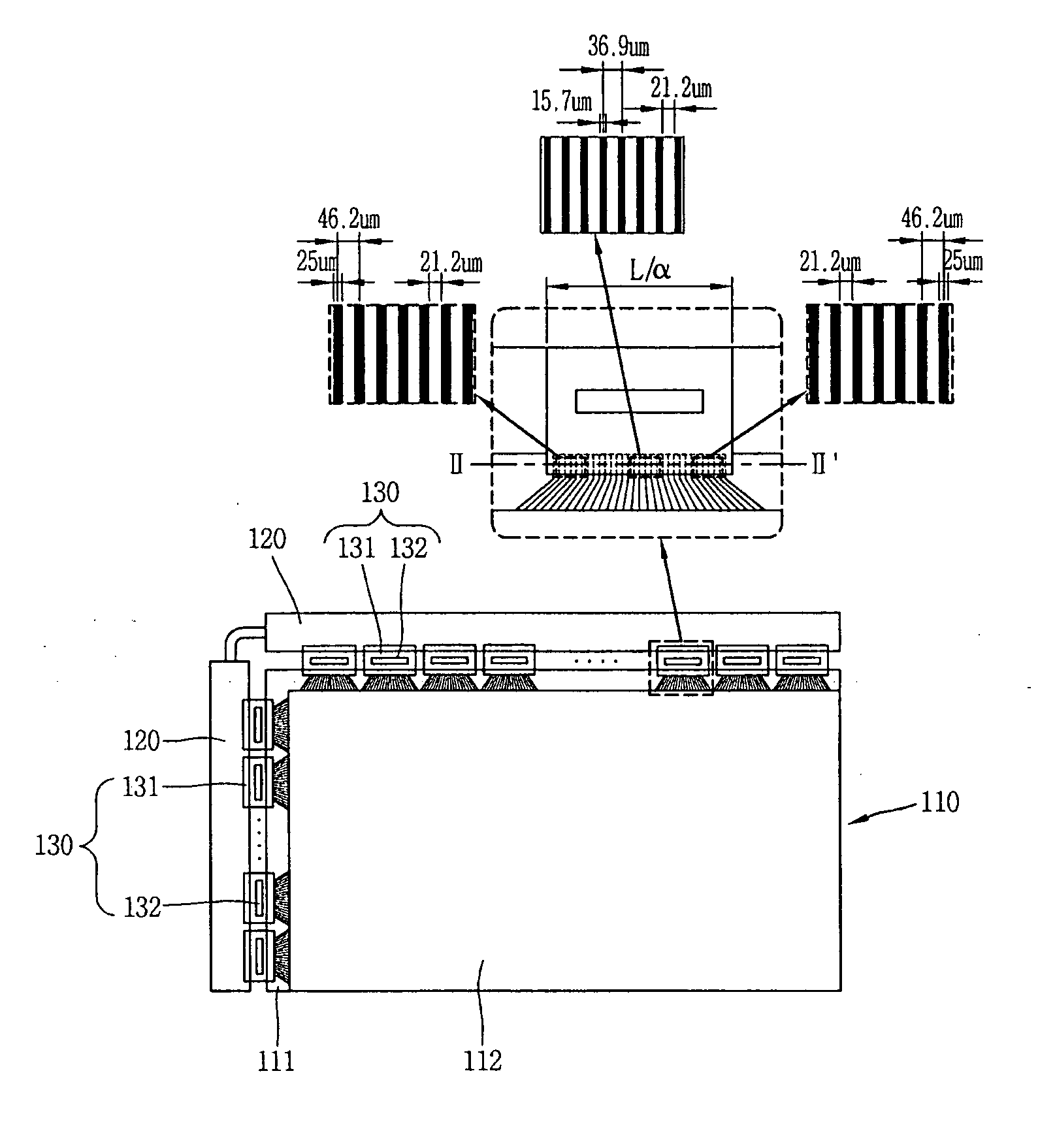
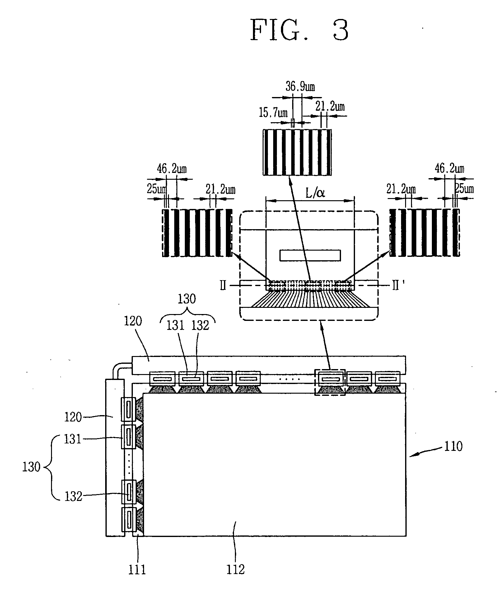
[0028]The structure of a liquid crystal display (LCD) and its fabrication method according to the present invention will now be described with reference to the accompanying drawings.

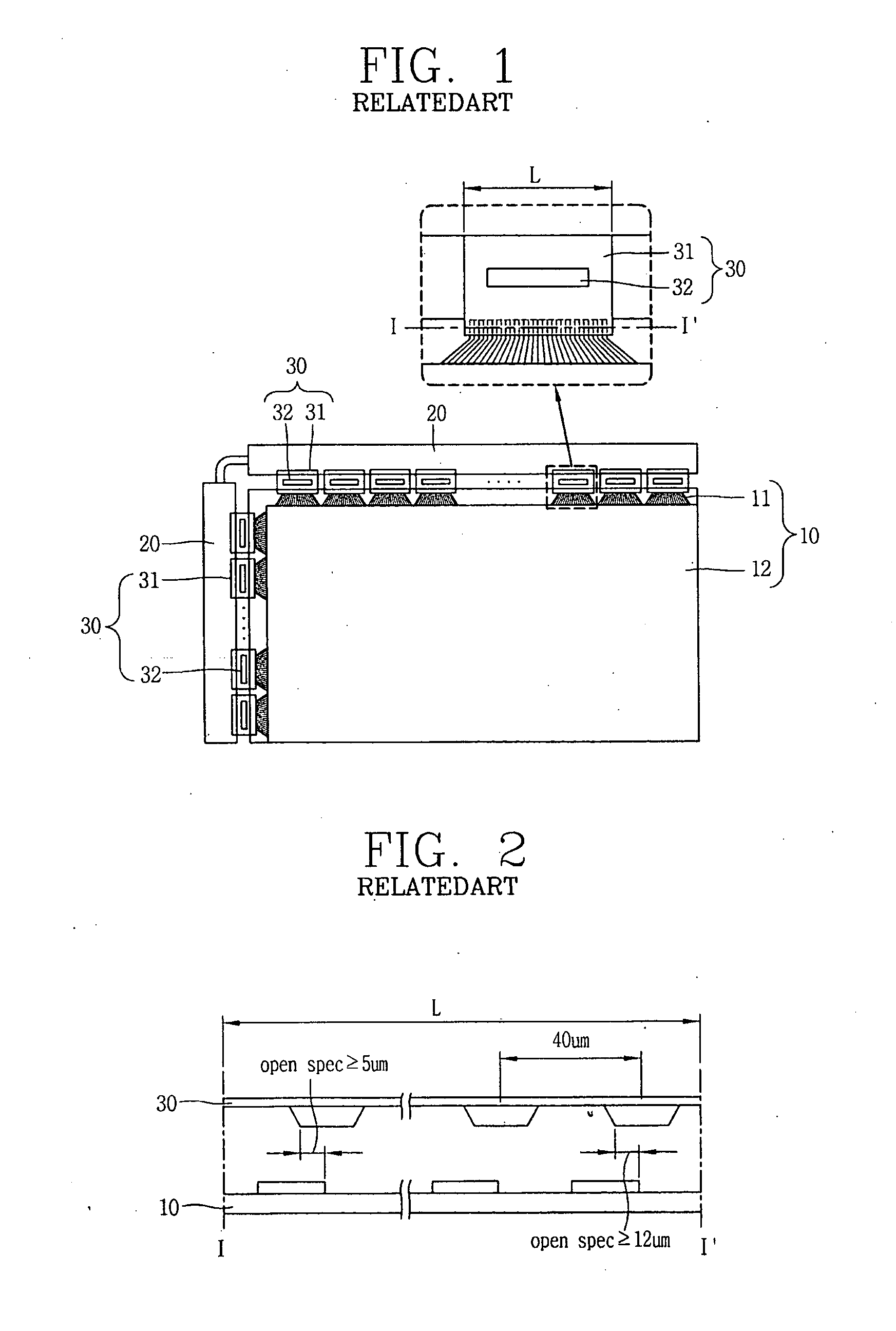
[0029]FIG. 3 shows the structure of an LCD according to an embodiment of the present invention, and FIG. 4 is a sectional view taken along line II-II′ of a pad part of a liquid crystal panel and a COF attached to the pad part in FIG. 3.

[0030]As shown in FIGS. 3 and 4, the LCD according to the present invention includes: a driving PCB (Printed Circuit Board) 120 that generates R, G and B data and control signals, a COF 130 attached on the driving PCB 120 and receiving signals; a liquid crystal panel 110 includes the COF 130 on edge region to receive signals to display an image, and a backlight (not shown) provided below the liquid crystal panel 110 and providing light. Here, the COF 130 includes input wirings attached to the driving PCB 120 and receiving data, output wirings formed to be separated from th...


PUM

PropertyMeasurementUnit
sizeaaaaaaaaaa
sizeaaaaaaaaaa
sizeaaaaaaaaaa

Abstract

A method for fabricating a liquid crystal display, includes: preparing a first substrate having a first region and a second region positioned at at least one side of the first region, and a second substrate attached to the first region of the first substrate; forming a plurality of gate lines and a plurality of data lines such that they cross each other to define unit pixel regions on the first region of the first substrate, and forming switching elements at crossings of the gate lines and data lines; and extending the gate lines and the data lines of the first region to the second region of the first substrate to form a plurality of pads constituting at least one group, wherein the intervals between pads at every region constituting the single group are the same, and the pad width is different as it goes from the pad positioned at the center toward the outermost pad. When FCTs with a small width size (L / α), namely, a width size of 35 mm, having 642 channels, based on the 17-inch or 19-inch LCD, are attached, misalignment between the pads of the liquid crystal panel and the output wirings of the FCTs attached to the pads can be prevented, and accordingly, a defective LCD can be reduced.

Description

BACKGROUND OF THE INVENTION[0001]1. Field of the Invention[0002]The present invention relates to a liquid crystal display (LCD) and a fabricating method of an LCD capable of designing a fine pitch of a pad and an FCT (Film Carrier Tape) output line of a liquid crystal in applying an FCT such as a TCP (Tape Carrier Package), a COF (Chip On Film) or the like having 642 channels of a 35 mm size to a liquid crystal panel based on a liquid crystal display (LCD) of 17 inches or 19 inches, to thereby preventing the occurrence of a short phenomenon due to misalignment of the liquid crystal panel and the FCT.[0003]2. Description of the Related Art[0004]As the Information Age advances, demands for display devices are increasing in various forms, and various flat panel display devices such as LCDs, PDPs (Plasma Display Panels), ELDs (Electro Luminescent Displays), VFDs (Vacuum Fluorescent Displays), or the like, have been studied, some of which have been utilized as display devices in various ...

Claims


Application Information

Patent Timeline
Patent Type & Authority Applications(United States)
IPC IPC(8): G02F1/1345G02F1/13
CPCG02F1/13452H05K2201/094H05K3/361H05K1/117G02F1/1345
Inventor KANG, JEONG-HO
Owner LG DISPLAY CO LTD
Why Eureka
Try Eureka