Array type capacitance sensor
- Summary
- Abstract
- Description
- Claims
- Application Information
AI Technical Summary
Benefits of technology
Problems solved by technology
Method used
Image

Examples
embodiment 1
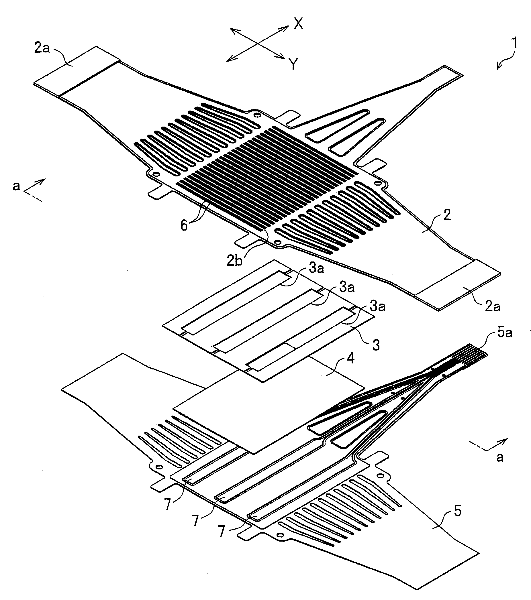
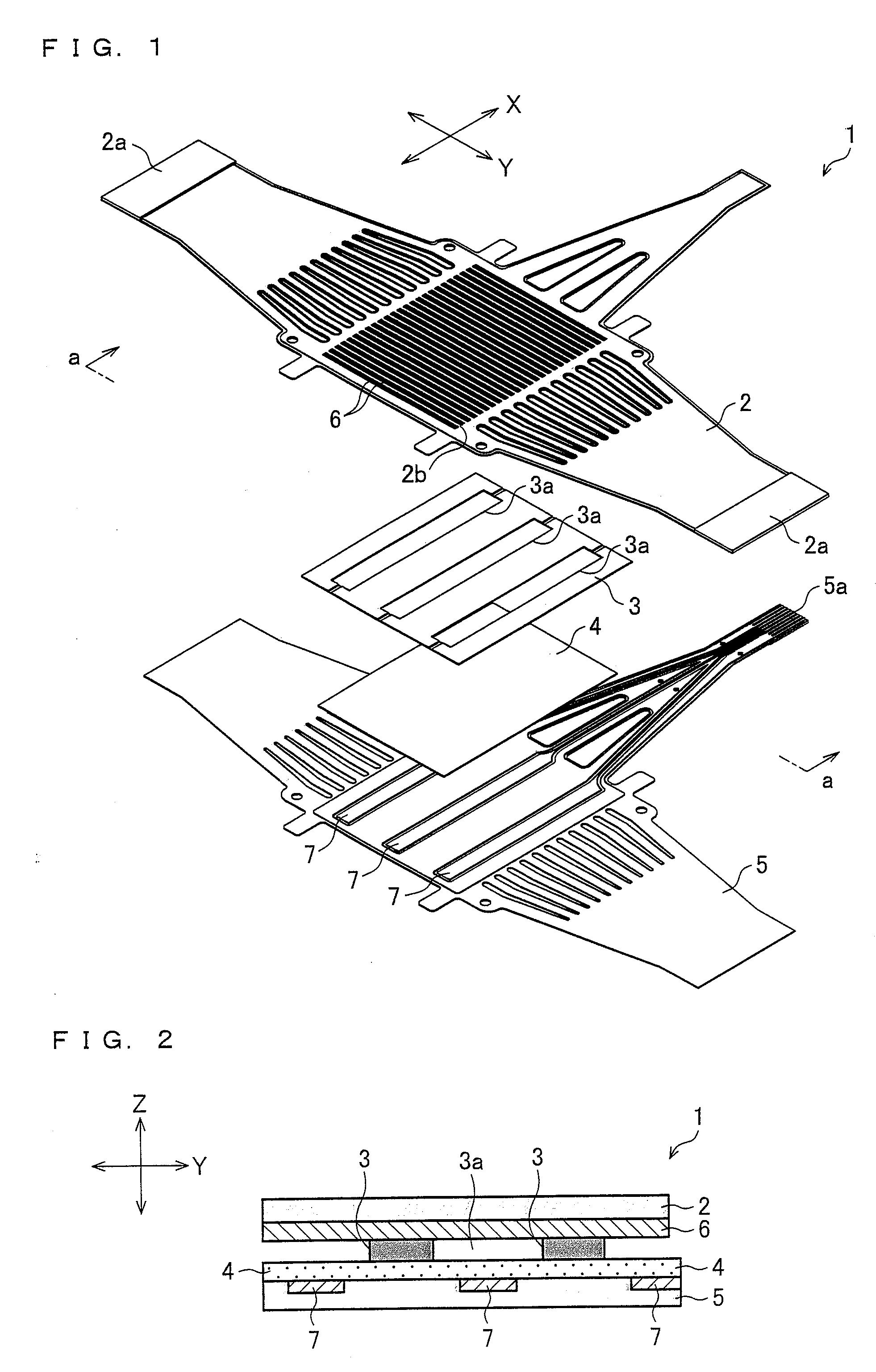
[0091]FIG. 1 is an exploded perspective view of an array type capacitance sensor according to Embodiment 1 of the present invention. FIG. 2 is a partial sectional view of the array type capacitance sensor, taken along the line a-a of FIG. 1. As illustrated in FIGS. 1 and 2, an array type capacitance sensor 1 includes: a movable-electrode-side substrate 2; a spacer 3; a dielectric film 4; and a fixed-electrode-side substrate 5.
[0092]The movable-electrode-side substrate (first substrate, second substrate) 2 is brought into contact with a target surface to be detected (in the present embodiment, a body surface of a living body) so as to receive intra-arterial pressure. The movable-electrode-side substrate 2 includes movable electrodes (first electrodes, second electrodes) 6, and connector connection sections 2a. The movable electrodes 6 are flexible and have a sheet shape. The movable electrodes 6 are provided on a side of the movable-electrode-side substrate 2 which side is opposite f...
embodiment 2
[0127]The following description deals with Embodiment 2 of the present invention with reference to FIGS. 15 and 16. It should be noted that, for convenience of explanation, same members in Embodiment 2 as those in Embodiment 1 are assigned the same reference numerals and the description of the members is omitted.
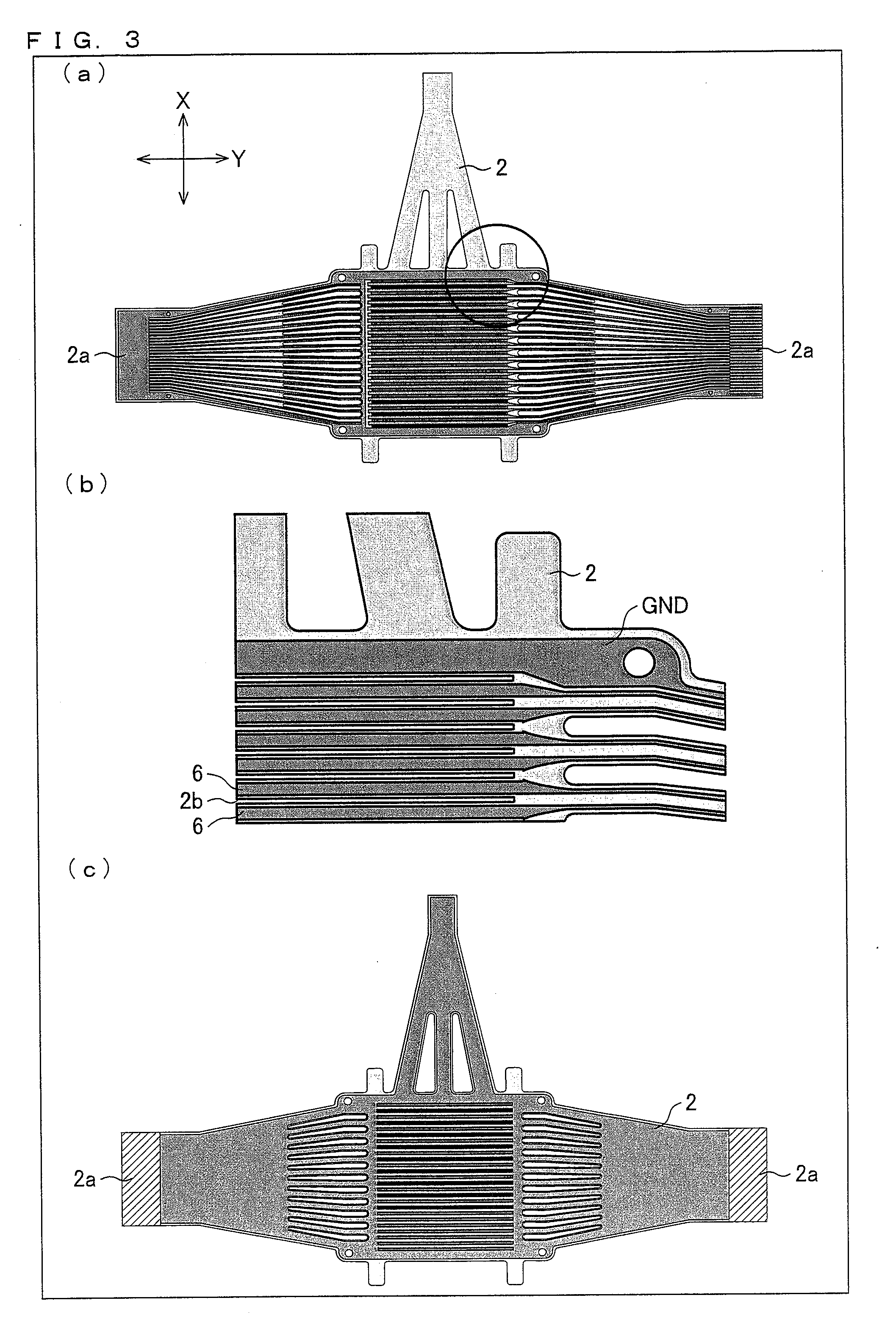
[0128]FIG. 15 is an exploded perspective view of an array type capacitance sensor 20 according to Embodiment 2 of the present invention. The array type capacitance sensor 20 of the present embodiment is different from the array type capacitance sensor 1 of Embodiment 1 in that the spacer 3 is improved.
[0129]FIG. 16 is a view schematically illustrating how a spacer 3 is arranged in the present embodiment. In FIG. 16, (a) is a plan view of the spacer 3, and (b) is a perspective view of the spacer 3. As illustrated in FIG. 16, the spacer 3 is provided with opening sections 3a for the three columns of fixed electrodes 7 so as not to cover the fixed electrodes 7 on the fixed elec...
embodiment 3
[0132]The following description deals with Embodiment 3 of the present invention with reference to FIGS. 17 through 19. It should be noted that, for convenience of explanation, same members in Embodiments 3 as those in Embodiments 1 and 2 are assigned the same reference numerals and the description of the members is omitted.
[0133]FIG. 17 is an exploded perspective view of an array type capacitance sensor 30 according to Embodiment 3 of the present invention. FIG. 18 is a view schematically illustrating an arrangement of the array type capacitance sensor 30 of the present embodiment, (a) is a top plan view of the movable-electrode-side substrate 2 of the array type capacitance sensor 30, (b) is a bottom plan view of the fixed-electrode-side substrate 5 of the array type capacitance sensor 30, and (c) is a cross-sectional view of the array type capacitance sensor 30, taken along the line a-a shown in (a). The array type capacitance sensor 30 of the present embodiment further includes ...
PUM
 Abstract
Description
Claims
Application Information
 - Generate Ideas
- Intellectual Property
- Life Sciences
- Materials
- Tech Scout
- Unparalleled Data Quality
- Higher Quality Content
- 60% Fewer Hallucinations
Browse by: Latest US Patents, China's latest patents, Technical Efficacy Thesaurus, Application Domain, Technology Topic, Popular Technical Reports.
© 2025 PatSnap. All rights reserved.Legal|Privacy policy|Modern Slavery Act Transparency Statement|Sitemap|About US| Contact US: help@patsnap.com