Fault detection apparatuses and methods for fault detection of semiconductor processing tools

a technology of fault detection and semiconductor processing, applied in the field of semiconductor processing, can solve the problems of consuming a lot of time, wafers and other resources, and unable to find the source of aluminum particles using the present troubleshooting method,

Active Publication Date: 2009-06-18
NOVELLUS SYSTEMS
View PDF9 Cites 33 Cited by
  • Summary
  • Abstract
  • Description
  • Claims
  • Application Information

AI Technical Summary

Problems solved by technology

However, because a large percentage of the tool may consist of aluminum, it is very time consuming to find the source of the aluminum particles using present troubleshooting methods.
However, between testings the fault may become catastrophic, that is, an unacceptable number of production wafers may become contaminated or otherwise damaged.
However, these and other methods consume a lot of time, wafers and other resources, and in many cases are not successful.
If unsuccessful, then wholesale replacement of multiple components may be required to identify and resolve the problem.
The longer the production tool is out of operation, the more costly the problem becomes.

Method used


Image

  • Fault detection apparatuses and methods for fault detection of semiconductor processing tools
  • Fault detection apparatuses and methods for fault detection of semiconductor processing tools
  • Fault detection apparatuses and methods for fault detection of semiconductor processing tools

Examples


Embodiment Construction

[0014]The following detailed description of the invention is merely exemplary in nature and is not intended to limit the invention or the application and uses of the invention. Furthermore, there is no intention to be bound by any theory presented in the preceding background of the invention or the following detailed description of the invention.

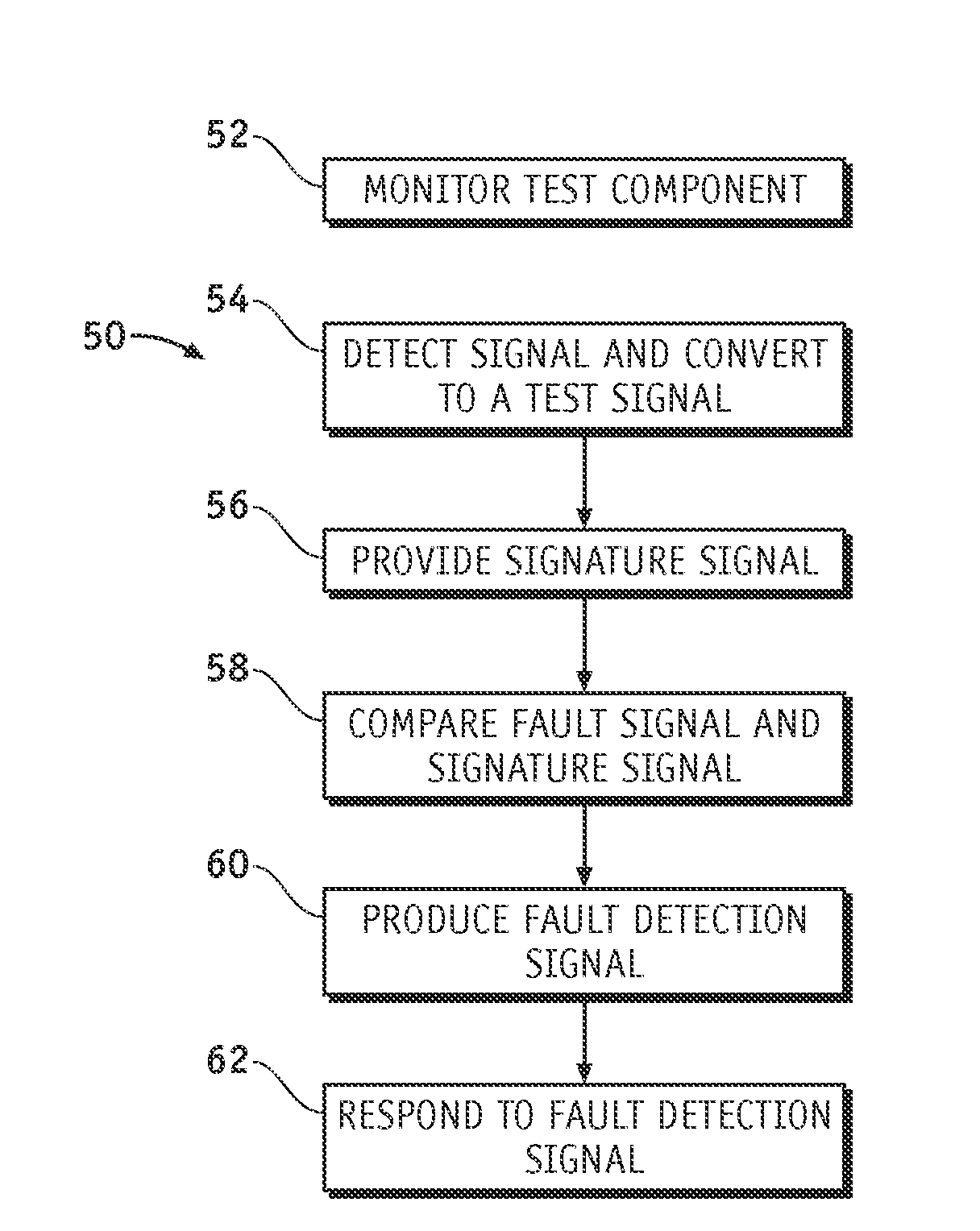
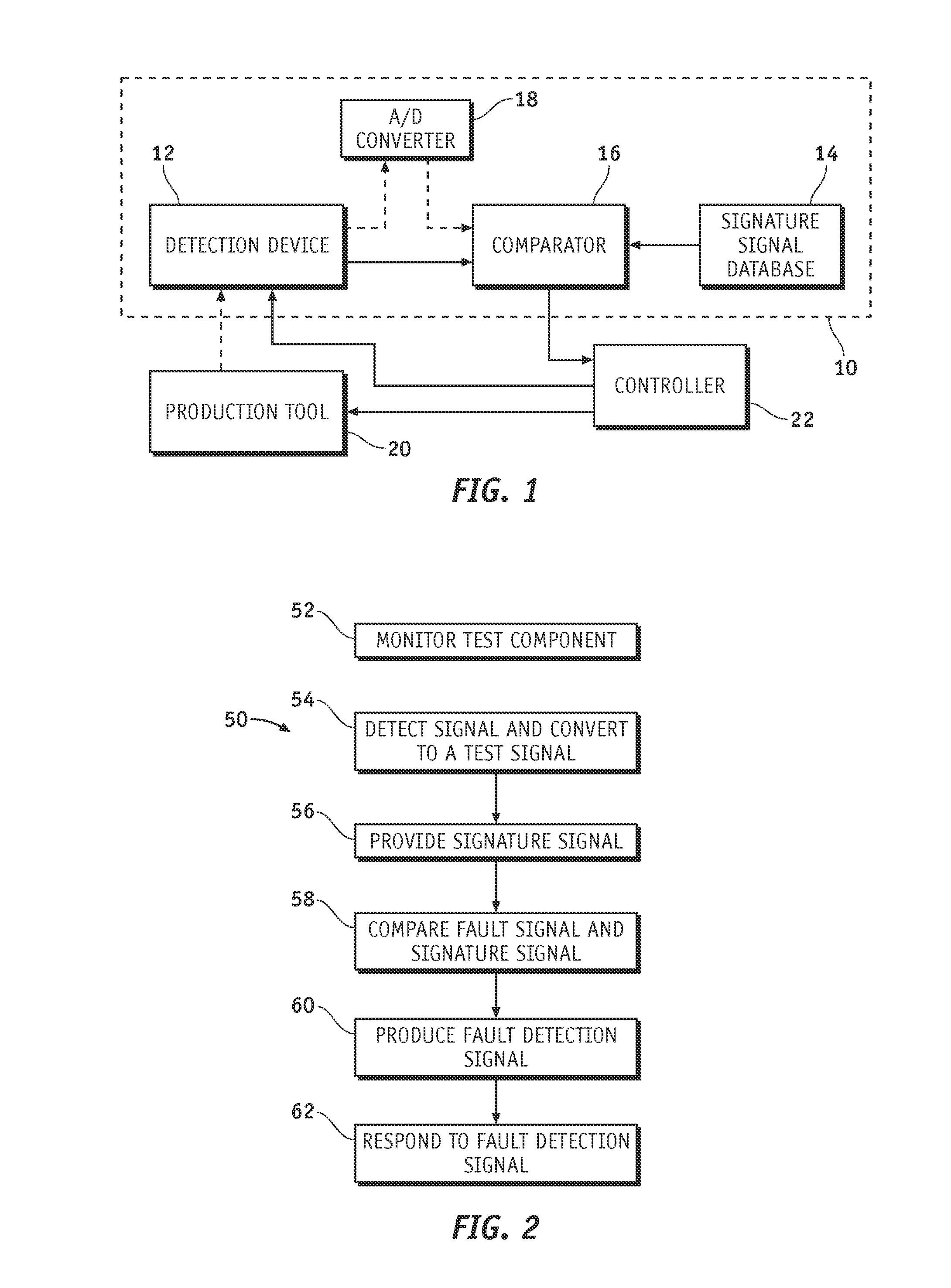
[0015]Referring to FIG. 1, in accordance with an exemplary embodiment of the present invention, a fault detection apparatus 10 is configured for the monitoring of a semiconductor wafer or IC (integrated circuit) fabricating or processing tool, hereinafter referred to as “production tool”, 20 and indicating when a fault in the operation of that tool has occurred. The production tool 20 may comprise any suitable fabrication or processing tool, such as, for example, a cleaning tool, a strip or etch tool, a vapor deposition tool, a sputtering tool, an electroplating tool, an annealing tool, a chemical mechanical polishing (CMP) tool, a wafer han...


PUM


Abstract

Fault detection apparatuses and methods for detecting a processing or hardware performance fault of a semiconductor production tool have been provided. In an exemplary embodiment, a method for detecting a fault of a semiconductor production tool comprises sensing a signal associated with a test component of the production tool during operation of the production tool and converting the signal to an electronic test signal. A prerecorded signature signal corresponding to the test component is provided and the test signal and the prerecorded signature signal are compared.

Description

FIELD OF THE INVENTION[0001]The present invention generally relates to semiconductor processing, and more particularly relates to fault detection apparatuses and methods for detecting processing or hardware performance faults of semiconductor processing tools.BACKGROUND OF THE INVENTION[0002]The ability to quickly determine the root cause of processing faults, such as particle contamination, film non-uniformity, wafer placement errors or other faults, in the production of a semiconductor wafer is confounded by the number of possible defect sources and the random wafer paths within the tool. For example, it is not uncommon to find aluminum particles on periodic particle qualification monitor wafers after processing in a semiconductor processing tool. However, because a large percentage of the tool may consist of aluminum, it is very time consuming to find the source of the aluminum particles using present troubleshooting methods.[0003]One present-day method for detecting faults in th...

Claims


Application Information

Patent Timeline
Patent Type & Authority Applications(United States)
IPC IPC(8): G01R31/02
CPCG05B23/0229G05B2219/31356G05B2219/37224H01L22/14H01L22/12G01R31/00G01R31/02H01L21/67288Y02P90/02
Inventor HANSEN, KEITH JOHN
Owner NOVELLUS SYSTEMS
Why Eureka
Try Eureka