

Antenna device
a technology of an antenna device and an antenna body, which is applied in the direction of antennas, antenna details, antenna couplings, etc., can solve the problems of affecting the isolation effect of signals, the degree of leakage or interference of waves or signals, and the inability to distinguish leakage signals from signals reflecting at objects, etc., and achieve good isolation
- Summary
- Abstract
- Description
- Claims
- Application Information
AI Technical Summary
Benefits of technology
Problems solved by technology
Method used
Image

Examples
first embodiment
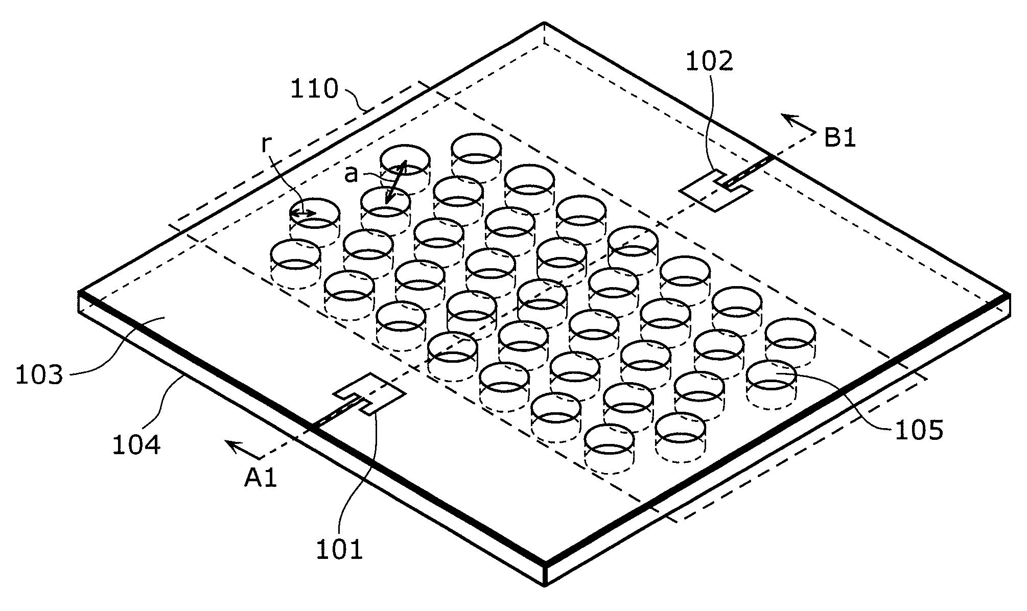
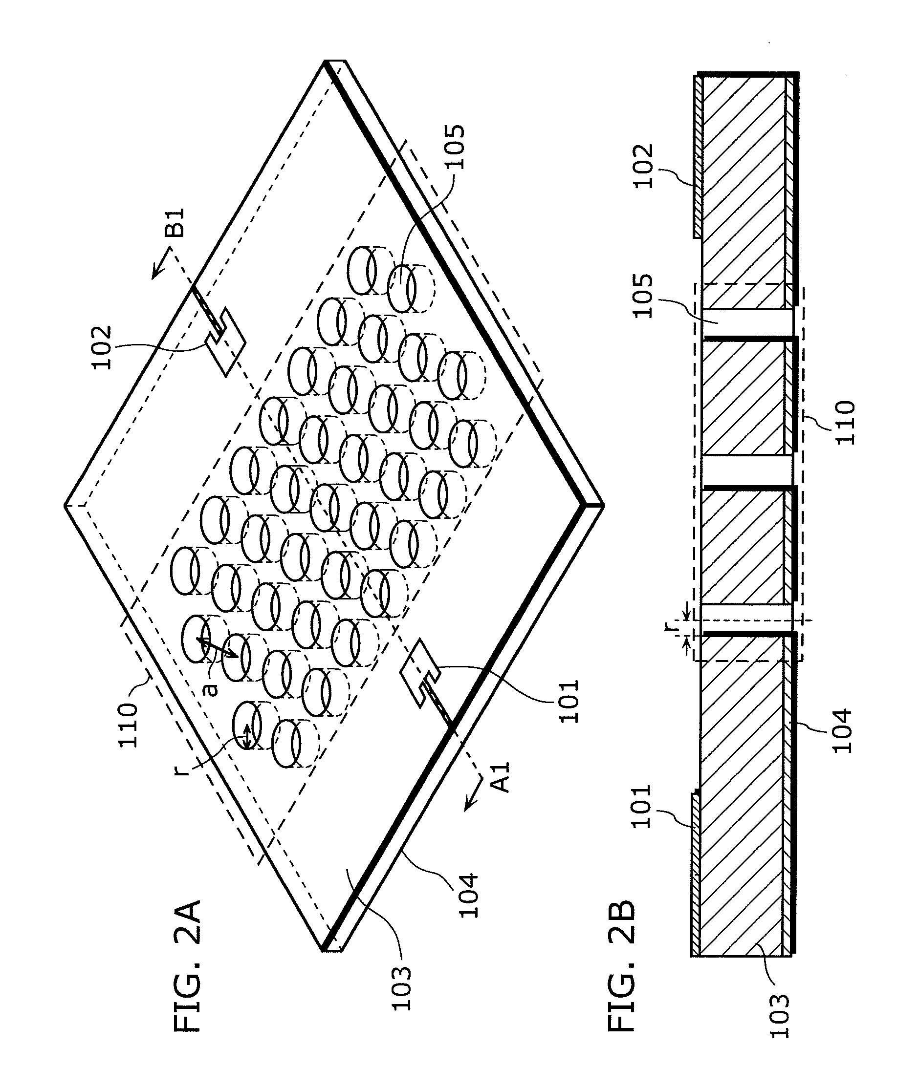
[0083]The antenna device according to the first embodiment can achieve good isolation between a transmission antenna and a receiving antenna, by forming a photonic crystal structure between the transmission antenna and the receiving antenna.
[0084]FIG. 2A is a perspective view of the antenna device according to the first embodiment of the present invention. FIG. 2B is a cross sectional view taken along line A1-B1 of FIG. 2A.
[0085]As shown in FIGS. 2A and 2B, the antenna device according to the first embodiment includes a substrate 103, a transmission antenna 101, a receiving antenna 102, a ground conductor 104, and a photonic crystal structure 110.
[0086]The substrate 103 is a monolayer substrate made of dielectric substance such as Teflon™.
[0087]The transmission antenna 101 is the first antenna element formed on a surface of the substrate 103, and transmits radio waves.
[0088]The receiving antenna 102 is the second antenna element formed on the surface of the substrate 103, and receiv...
second embodiment
[0110]In the antenna device according to the second embodiment, a photonic crystal structure is realized by filling each of the plurality of throughholes 105 of FIGS. 2A and 2B with a substance different from the substance of the substrate 103.
[0111]FIG. 4A is a perspective view showing a structure of the antenna device according to the second embodiment. FIG. 4B is a cross sectional view taken along line A2-B2 of FIG. 4A. Here, the same reference numerals of FIGS. 2A and 2B are assigned to identical elements of FIGS. 4A and 4B, so that the detailed explanation for the identical elements is not given again below.
[0112]As shown in FIGS. 4A and 4B, the antenna device according to the second embodiment includes a photonic crystal structure 310 having a plurality of throughholes 306.
[0113]The plurality of throughholes 306 are formed between the transmission antenna 101 and the receiving antenna 102. Each of the plurality of throughholes 306 is filled with a filling of a substance differ...
third embodiment
[0117]The antenna device according to the third embodiment can achieve high isolation between the transmission antenna and the receiving antenna, by further including a ground conductor formed on a surface of the substrate 103 in the antenna device according to the second embodiment.
[0118]FIG. 5A is a perspective view showing a structure of the antenna device according to the third embodiment. FIG. 5B is a cross sectional view taken along line A3-B3 of FIG. 5A. Here, the same reference numerals of FIGS. 4A and 4B are assigned to identical elements of FIGS. 5A and 5B, so that the detailed explanation for the identical elements is not given again below.
[0119]The antenna device shown in FIGS. 5A and 5B differs from the antenna device according to the second embodiment in including the a top surface conductor 407 and a connection conductor 408.
[0120]The top surface conductor 407 is formed on a surface of the substrate 103 between the transmission antenna 101 and the receiving antenna 10...
PUM
 Abstract
Description
Claims
Application Information