Image display apparatus

a technology of image display and display screen, which is applied in the direction of electrical apparatus casings/cabinets/drawers, television systems, instruments, etc., can solve the problems of distortion resulting from the difference between thermal expansion of the substrate, deterioration of image quality, and distortion of the substrate resulting from the difference between thermal expansion and the substrate, etc., to prevent a position shift and suppress the effect of distortion generated

Inactive Publication Date: 2009-06-18
CANON KK
View PDF12 Cites 5 Cited by
  • Summary
  • Abstract
  • Description
  • Claims
  • Application Information

AI Technical Summary

Benefits of technology

[0007]Then, the present invention aims to provide an image display apparatus which can achieve both of prevention of a position shift between substrates and suppression of distortion generated in the substrates.

Problems solved by technology

Usually, although each substrate is formed with glass as a base material, distortion resulting from difference between thermal expansions of substrates may arise in each substrate by factors, such as a temperature difference between one substrate and another substrate which arises at the time of use.
When both of the substrates generate a relative position shift, there is a possibility that an electron beam emitted from an electron source may be radiated in a position shifting from a desired position of an image display unit, and may cause deterioration of image quality by this distortion.
The reinforcing structure disclosed in Japanese Patent Application Laid-Open No. 2004-087475 is effective in order to prevent a position shift between both substrates, but since the substrates are restrained mutually, distortion resulting from the difference between thermal expansions may arise in the substrates.
When the distortion arises in the substrates, even if the position shift between the substrates is prevented, breakdown of the substrate may be caused and there is a possibility of reducing reliability as an image display apparatus.

Method used


Image

  • Image display apparatus
  • Image display apparatus
  • Image display apparatus

Examples


first embodiment

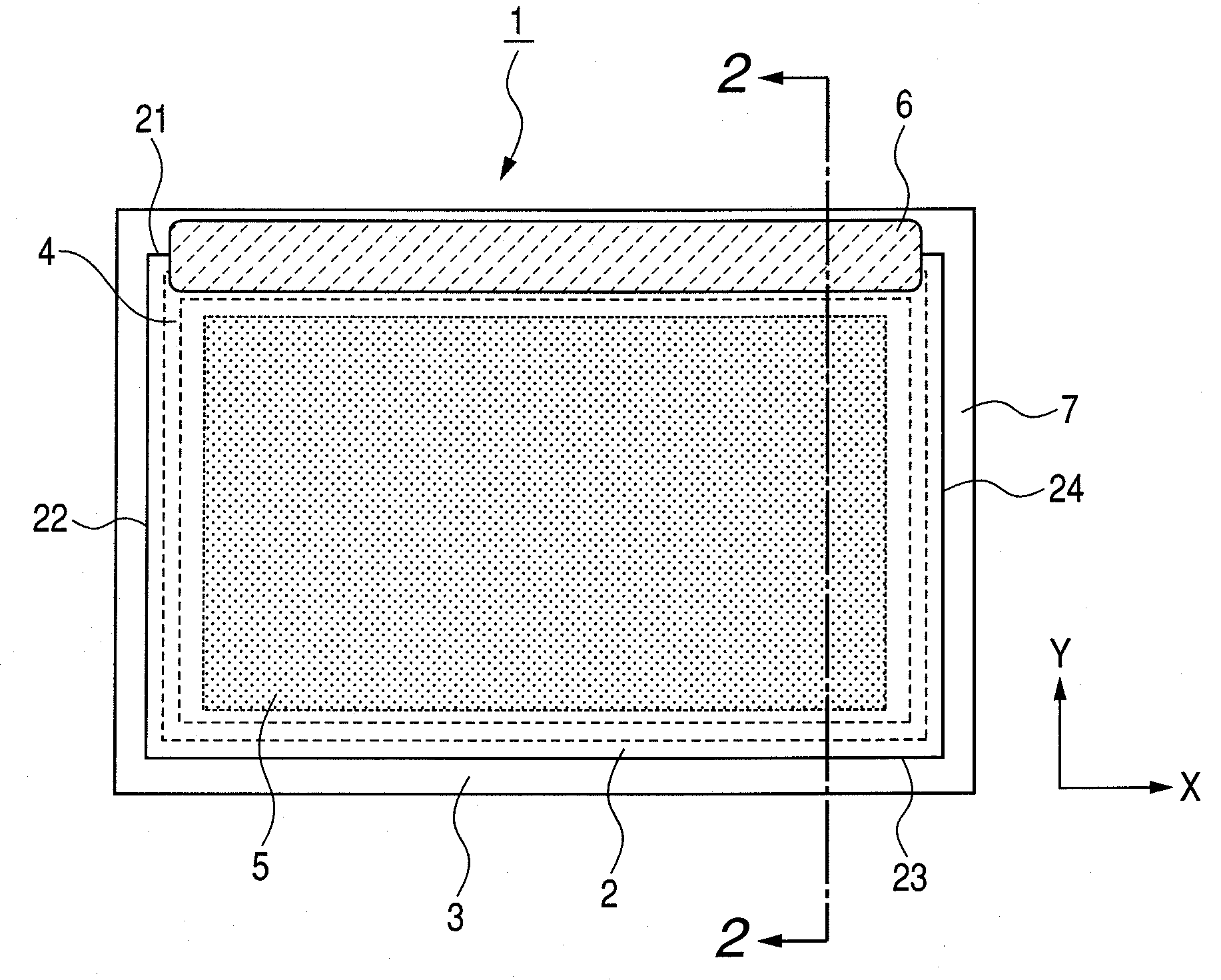
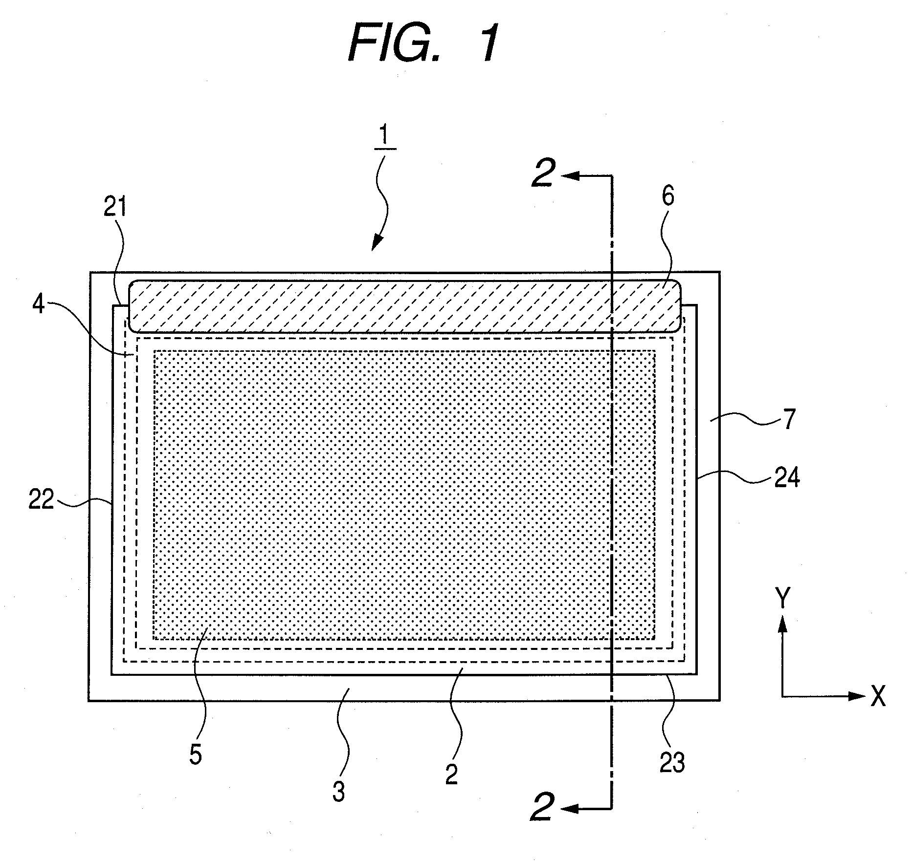
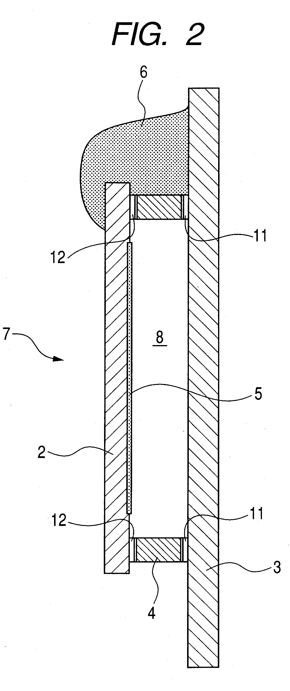
[0016]FIGS. 1 and 2 are a front view of an image display apparatus illustrating a first embodiment of the present invention, and a sectional view along line 2-2 in FIG. 1, respectively. The first embodiment is the image display apparatus in which a surface conduction electron-emitting device is used.

[0017]The first substrate 2 includes an image display unit 5 including a phosphor (not illustrated) and the like. The second substrate 3 includes an electron-emitting source (not illustrated), and is provided with being placed in opposition to the first substrate 2. From the electron-emitting source, electrons are emitted according to an image signal, and collide with the phosphor, the phosphor emits light, and a desired image is displayed. A space 8 is formed between the first substrate 2 and the second substrate 3. The first substrate 2 and the second substrate 3 are bonded through an outer frame 4, and construct an envelope 7 whose interior is made into a vacuum. Since the first subst...

second embodiment

[0023]FIGS. 3 and 4 are a front view of an image display apparatus illustrating a second embodiment of the present invention, and a sectional view along line 4-4 in FIG. 3, respectively. Although being the image display apparatus which uses a field emission device, the second embodiment is also applicable similarly to another image display apparatus, such as an image display apparatus using a surface conduction electron-emitting device, or a liquid crystal display. The second embodiment is the same as the first embodiment except construction and an installation method of a position fixing member differing from the first embodiment besides this point.

[0024]In this embodiment, position fixing members 6a and 6b are provided so as to connect the first substrate 2a and the second substrate 3a to only parts of two sides 21a and 24a of the envelope 7a being adjacent to each other. The position fixing members 6a and 6b are metal members made of an Fe-47Ni alloy, and are bonded with the subs...


PUM


Abstract

An image display apparatus is provided to achieve both of position shift prevention between substrates and suppression of distortion generated in the substrates. An image display apparatus has an envelope including a first substrate provided with an image display unit, a second substrate placed in opposition to the first substrate, and a bonding member for hermetically seal bonding the first substrate to the second substrate so as to form a space between the first and second substrates. The image display apparatus further has a position fixing member which is bonded with both of the first and second substrates along one side of an outer periphery of the envelope, and suppresses a position shift between the first and second substrates.

Description

BACKGROUND OF THE INVENTION[0001]1. Field of the Invention[0002]The present invention relates to an image display apparatus, and in particular, to a bonding structure between substrates of an image display apparatus.[0003]2. Description of the Related Art[0004]An image display apparatus using a surface conduction electron-emitting device or a field emission electron-emitting device is known. In this kind of image display apparatus, a substrate in which an image display unit is formed, and a substrate in which an electron-emitting source is formed are arranged oppositely, and structure in which these substrates are bonded through an outer frame is common. Specifically, the outer frame is firmly fixed to one side of a substrate with frit (low melting point glass), the outer frame and another side of the substrate are sealed with a bonding member, and an envelope is formed. As the bonding member, a low melting point metal, such as In (indium), is used. A space between substrates, that ...

Claims


Application Information

Patent Timeline
Patent Type & Authority Applications(United States)
IPC IPC(8): H04N5/645
CPCH01J9/261H01J31/127H01J31/123H01J29/16
Inventor KAMIGUCHI, KINYA
Owner CANON KK
Why Eureka
Try Eureka