Power semiconductor component with trench-type field ring structure

a technology of trench-type field rings and semiconductor components, applied in semiconductor devices, basic electric elements, electric devices, etc., can solve problems such as contamination risks, and achieve the effect of avoiding contamination in wide regions of diffusion profiles and shortening diffusion tim

Inactive Publication Date: 2009-07-16
SEMIKRON ELECTRONICS GMBH & CO KG
View PDF4 Cites 0 Cited by
  • Summary
  • Abstract
  • Description
  • Claims
  • Application Information

AI Technical Summary

Benefits of technology

[0006]It is an object of the invention to provide a power semiconductor component with a field ring structure, while avoiding contamination in wide regions of the diffusion profile, and a method for producing such a component having a shorter diffusion time than heretofore.

Problems solved by technology

Since a deep diffusion of the dopant is necessary here, long diffusion times are also necessary, which risks contamination, for example by heavy metals, of the diffusion zone.

Method used


Image

  • Power semiconductor component with trench-type field ring structure
  • Power semiconductor component with trench-type field ring structure
  • Power semiconductor component with trench-type field ring structure

Examples


Embodiment Construction

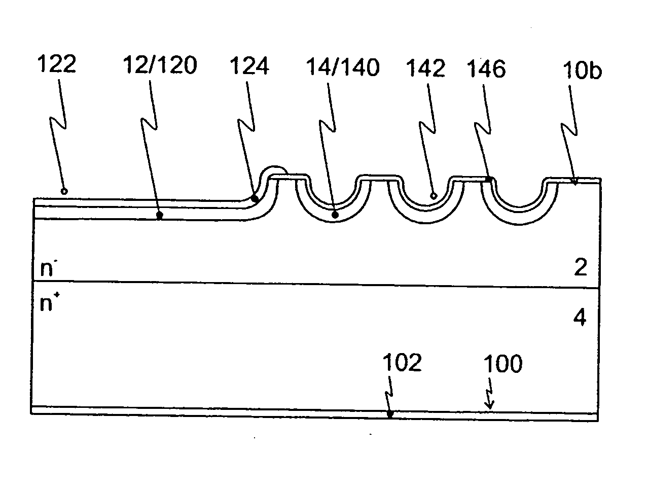
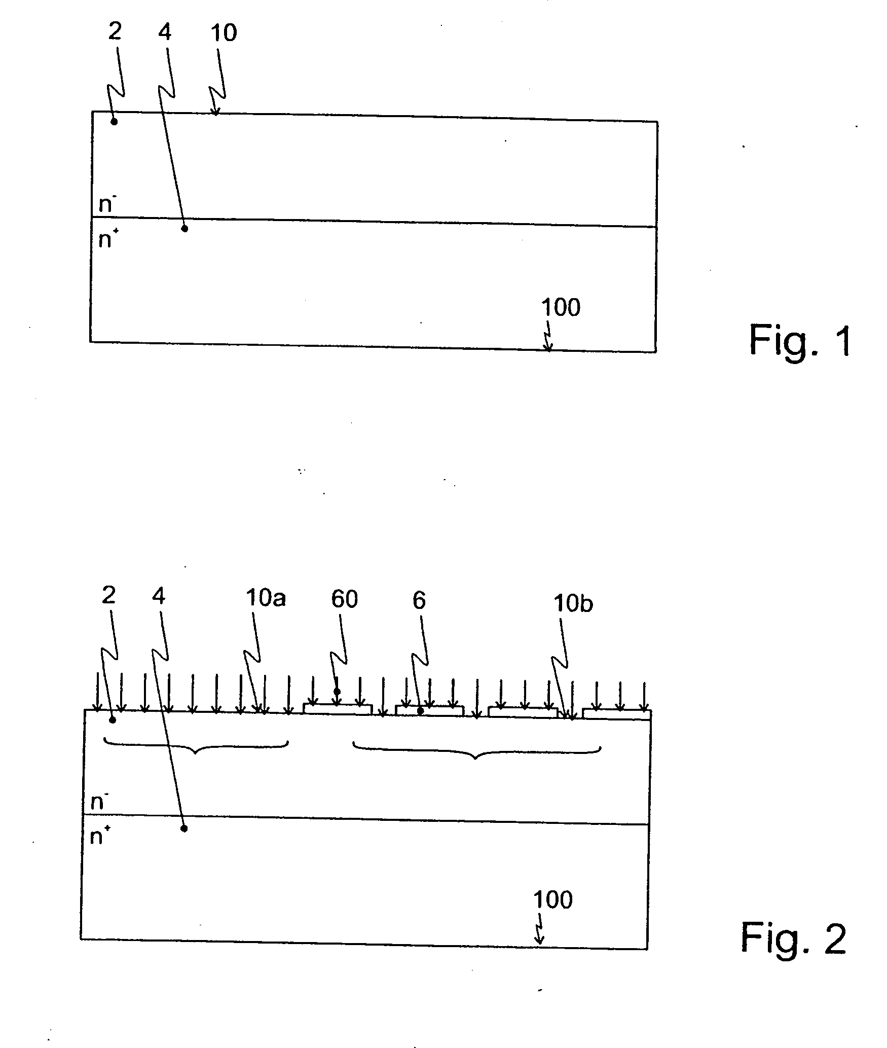
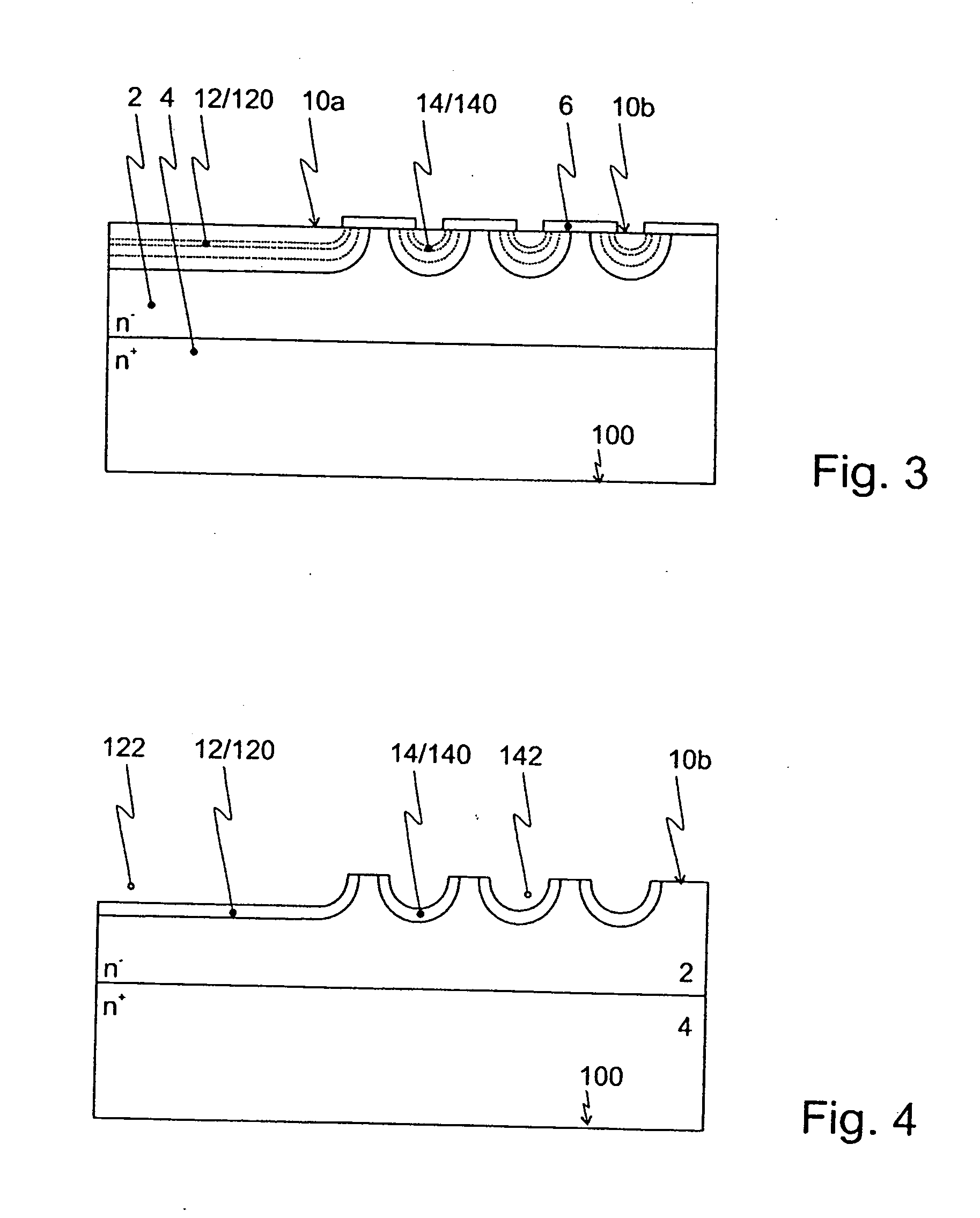
[0025]FIG. 1 shows an excerpt—not to scale—from a base body 2, 4 of a power semiconductor component according to the invention, by way of illustrative example, a power diode for a reverse voltage of 1200 V. This example is also maintained in principle for the following figures. Base body 2, 4 has an n-type doping having two different concentrations. A weakly doped region 2 is adjacent to a first surface 10 of the body, while a heavily doped region 4 is adjacent to a second surface 100. The boundary of the two dopings runs in the interior of the base body parallel to surfaces 10, 100.

[0026]FIG. 2 shows the partial step, of a first preferred method for forming doping profiles having a second doping, both for the contact region and for the field ring structure. In accordance with the prior art, various regions are masked 6 here in preparation for the selective doping. The contact region will be developed in the region of a first partial area 10a, and the field rings of the field ring s...


PUM


Abstract

A power semiconductor component and a method for producing such a component. The component comprises a semiconductor base body having a first doping. A pn junction is formed in the base body by a contact region having a second doping with a first doping profile. A field ring structure has a second doping with a second doping profile. The contact region and the field ring structure are arranged at respectively assigned first and second partial areas of a first surface of the base body. Both extend into the base body, wherein the base body has, for the field ring structure, a trench-type cutout assigned to each respective field ring, the surface of said cutout following the contour of the assigned doping profile.

Description

BACKGROUND OF THE INVENTION[0001]1. Field of the Invention[0002]The invention is directed to a power semiconductor component, preferably a power diode, having at least one pn junction and a reverse voltage strength of at least 600 V, for applications in power class converters. Power semiconductor components of this type have an edge region which contributes to the reverse voltage strength.[0003]2. Description of the Related Art[0004]Some known power semiconductor components include a concentric structure composed of a plurality of field rings in an edge region thereof. In this case, it is known to produce said field rings by diffusion, wherein a dopant is applied in masked fashion on the surface and subsequently diffused into the semiconductor body by heating, thereby forming a diffusion profile. For bulk-conductive power semiconductor components, it is customary to form the field rings together with the production of a pn junction that represents the active (current-carrying) regio...

Claims


Application Information

Patent Timeline
Patent Type & Authority Applications(United States)
IPC IPC(8): H01L29/66H01L21/04
CPCH01L29/417H01L29/8611H01L29/66128
Inventor KONIG, BERNHARD
Owner SEMIKRON ELECTRONICS GMBH & CO KG
Why Eureka
Try Eureka