Time-balanced multiplexer switching methods and apparatus
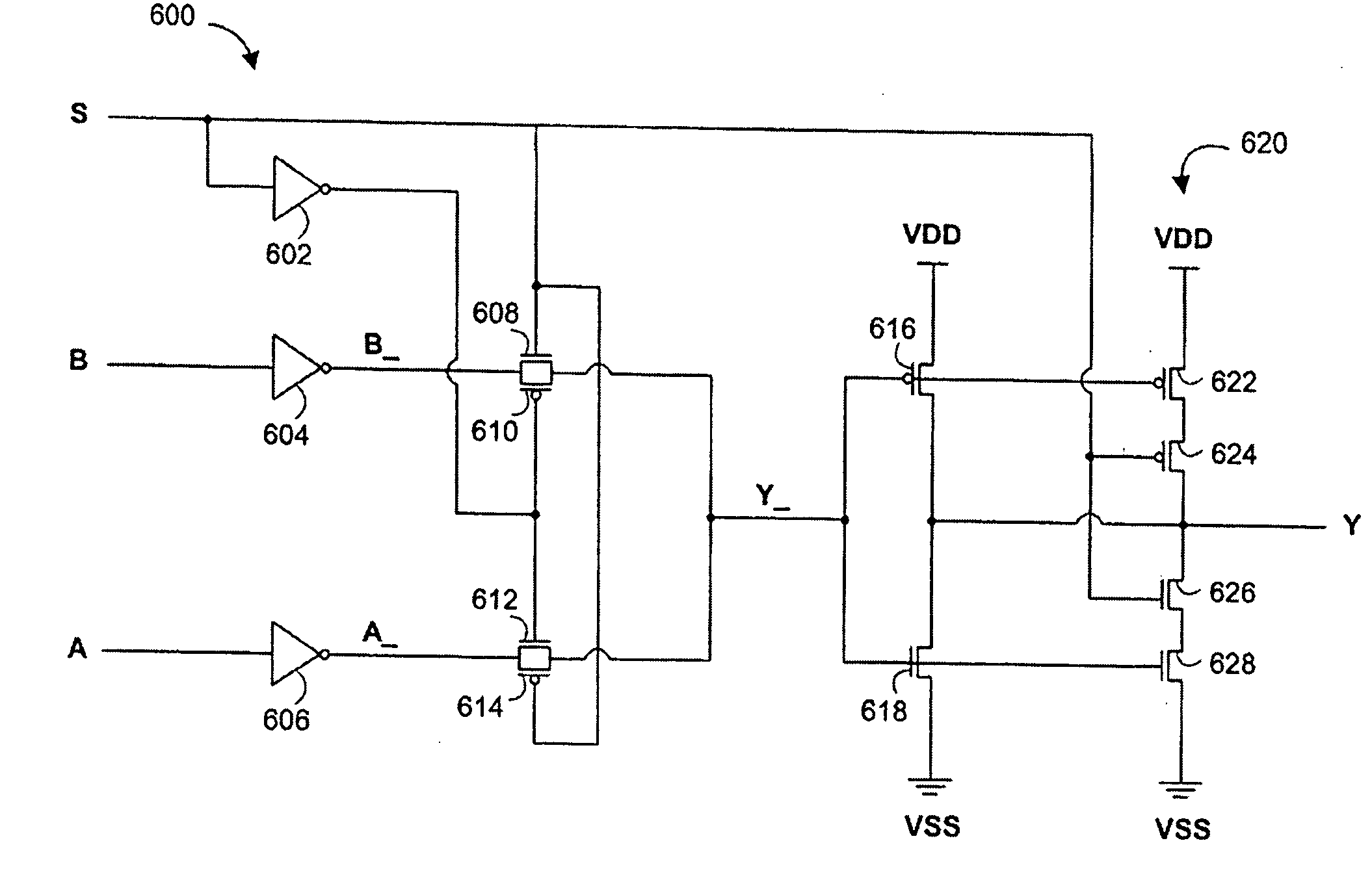
a multiplexer and switching method technology, applied in logic circuits, electric pulse generators, instruments, etc., can solve the problem of substantial equal delay before the corresponding output signal, and achieve the effect of time-balanced multiplexer switching
- Summary
- Abstract
- Description
- Claims
- Application Information
AI Technical Summary
Benefits of technology
Problems solved by technology
Method used
Image
Examples
Embodiment Construction
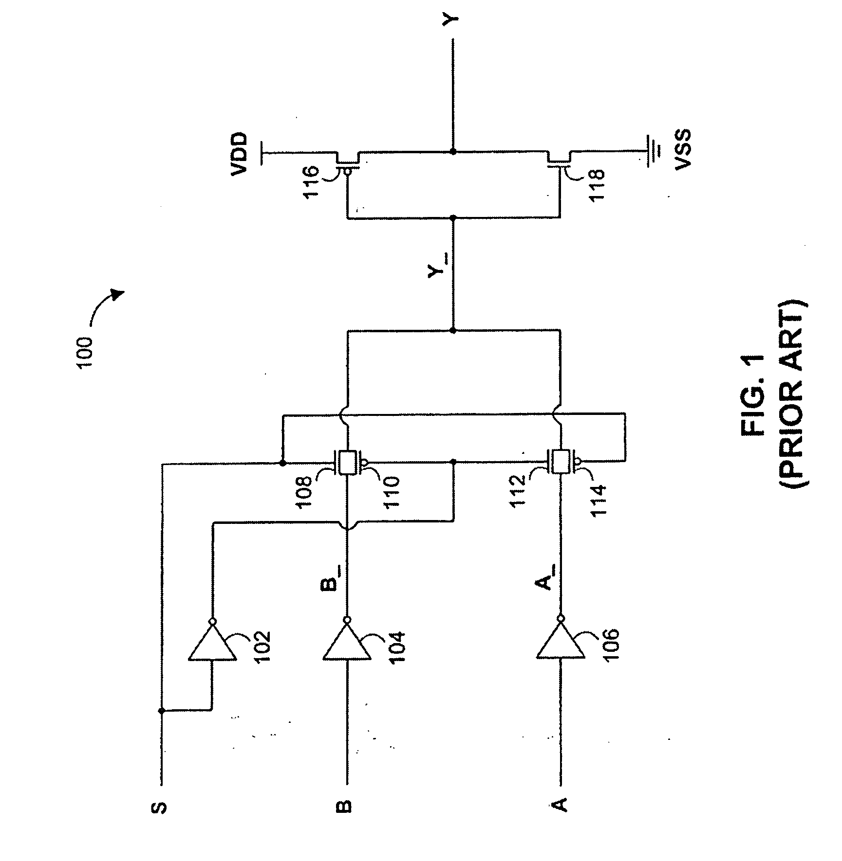
[0021]FIG. 1 is a circuit diagram of an illustrative multiplexer 100 that exhibits unbalanced switching. Selector input S selects between data inputs B and A. The selected data input is passed to data output Y through two stages of inversion. Voltage references are provided by the power source (“VDD”) and ground (“VSS”).
[0022]Selector input S is coupled to the gates of N-type metal-oxide semiconductor (“NMOS”) transistor 108 and P-type metal-oxide semiconductor (“PMOS”) transistor 114. Selector input S is also coupled to inverter 102, whose output is coupled to the gates of PMOS transistor 110 and NMOS transistor 112. Thus, transistors 108, 110, 112, and 114 serve as pass-gates that are operated by selector input S and an inversion of selector input S.
[0023]When the voltage of selector input S reflects a logical 0, transistors 112 and 114 will be activated, while transistors 108 and 110 will be deactivated. Accordingly, the logical value carried by data input A will be inverted by i...
PUM
 Abstract
Description
Claims
Application Information


