Embedded NANO UV blocking barrier for improved reliability of copper/ultra low k interlevel dielectric electronic devices

a technology of inter-layer dielectric electronic devices and nano-uv blocking, which is applied in the direction of semiconductor devices, semiconductor/solid-state device details, electrical apparatus, etc., can solve the problems of reducing the size of the device, reducing the dielectric constant, and no longer satisfying the requirements of aluminum, so as to reduce the dielectric constant, prevent uv/e-beam modification, and minimize stress changes

Inactive Publication Date: 2008-05-29
GLOBALFOUNDRIES INC
View PDF22 Cites 56 Cited by
  • Summary
  • Abstract
  • Description
  • Claims
  • Application Information

AI Technical Summary

Benefits of technology

[0033]A primary advantage of the present invention is the prevention of UV / e-beam modification to cap layers by embedding a dielectric blocking layer within the cap barrier film. Methods for the utilization, compositions of matter, and structures that implement the barrier films are also described.
[0034]The present invention can be used in any microelectronic device that uses metal interconnects including, for example, high speed microprocessors, application specific integrated circuits, and memory storage. Use of a multilayered dielectric diffusion barrier layer of the present invention is extremely advantageous for use with integrated circuits that use low-k dielectrics that require UV cure.
[0035]In an embodiment of this invention, an interconnect includes the multi-film dielectric diffusion barrier layer comprised of two or more sub-films that exhibit minimal change in material and electronic properties with UV cure. At least one sub-film is a material having a high C content with a high optical bandgap, which can block UV from modifying the desired properties of the cap layer. At least another of these sub-films may be a CVD deposited film that is impermeable to air and a metal diffusion barrier. The UV blocking film can be placed atop and / or below, and / or in between laminated barrier films. Optionally, adhesion layers may be applied at any of the interfaces in the multi-film dielectric diffusion layer or at interfaces between the sublayers.
[0036]The multilayered dielectric diffusion barrier layer of the present invention can have a tunable dielectric constant, depending on the thickness of the embedded layer (2 to 10 nm). Composite dielectric constant values can range from (3<k<7), while maintaining the required metal diffusion and air barrier properties, and minimizing stress change by UV cure. In addition, the multilayered dielectric diffusion barrier is thermally stable to temperatures greater than 400° C. and can be dense (i.e., non-porous) or porous to further reduce the dielectric constant.
[0037]In a second embodiment of the present invention, a method for producing the multilayered dielectric diffusion barrier layer is described. The multilayered dielectric diffusion barrier layer of the present invention is generated atop an interconnect having exposed metal and dielectric features. Each sublayer is then deposited by either CVD related approaches, or by solvent based processes (e.g., spin coating). Optionally, adhesion promoters are applied at any interface of the multilayered dielectric diffusion barrier layer or at interfaces between the sublayers.
[0038]In a third embodiment of the present invention, compositions of the multilayered dielectric diffusion barrier layer and its sublayers are provided. At least one sublayer is produced by a CVD based process whereby the air and metal diffusion barrier sublayer is comprised of silicon nitride, silicon carbonitride, or a dielectric with the general composition of SitNuCvOwHx, where 0.1≦t≦0.8. 0≦u≦0.8, 0.05≦v≦0.8. 0≦w≦0.3, 0.05≦x≦0.8 for t+u+v+w+x=1. At least one other sublayer is produced by a CVD based process whereby the sublayer is comprised of UV blocking high band gap films such as boronitride, silicon boronitride, carbon boronitride, silicon carbon boronitride, and carbon films, or lower band gap films with better mechanical, electrical, and Cu diffusion properties such as nitrided carbon (CNx) and boron doped nitrided carbon (CBxNy).

Problems solved by technology

While aluminum-based metallurgies have been the material of choice for use as metal interconnects in the past, aluminum no longer satisfies requirements as circuit density and speeds for semiconductor devices increase and the scale of devices decreases.
Despite these advantages, there is the significant problem that copper diffuses readily into the surrounding dielectric material as processing steps continue.
However there is the problem that in a conventional HDP deposition process, a seam is formed in the HDP CVD cap layer, and a crack in the cap layer often develops at this seam due to stress within the structure.
If the crack develops in a portion of the cap layer overlying a copper conductor, the copper conductor may be readily exposed to moisture and other sources of oxygen.
If the crack develops in a portion of the cap layer overlying the ILD, the copper conductor may be exposed to moisture diffusing through the ILD.
Moreover, any crack in the cap layer may lead to copper diffusion into the ILD through the seam leading to formation of a copper nodule under the cap layer.
Such a copper nodule may lead to short circuits due to leakage of current between adjacent interconnect lines.
Another significant disadvantage occurs when HDP CVD films are integrated with low-k dielectric materials.
In more advanced ground-rule devices, PE CVD films have been found to be inferior to cap layers formed by other deposition techniques such as HDP CVD because of poor adhesion to the copper surface.
However, subsequent deposition of insulating layers onto the cap layer will produce stress which can cause the cap layer to peel from the copper surface.
This delamination results in several catastrophic failure mechanisms, including lifting interlayer dielectrics, lifting copper conductors, copper diffusion from uncapped copper lines, and electromigration.
Often the passivation layer must also function as an etch stop layer during subsequent processing, however materials which perform best as etch stop layers often do not perform best as passivation layers.
For example, silicon oxynitride, SiON, is useful as an etch stop layer but it is less desirable as a passivation layer because of delamination which can occur between copper and silicon oxynitride.
Wang et al describes a problem with a bilayer of a UVN / HDP nitride capping layer formed by an UVN film and an HDP nitride film, which is that in forming a via hole, the Reactive Ion Etching (RIE) process continues too deep and punches through the UVN film and lands on the HDP film.
If the UVN is completely missing under a via hole, the via RIE will reach down to the HDP nitride film, which results in problems.
A seam in the HDP nitride can become an ingress path for copper (Cu) to react with moisture, which leads to volume expansion and rupture of the capping layer.
The observed change in stress increases the dielectric (k) value of the cap layer and adversely impacts the mechanical integrity of the structure.

Method used


Image

  • Embedded NANO UV blocking barrier for improved reliability of copper/ultra low k interlevel dielectric electronic devices
  • Embedded NANO UV blocking barrier for improved reliability of copper/ultra low k interlevel dielectric electronic devices
  • Embedded NANO UV blocking barrier for improved reliability of copper/ultra low k interlevel dielectric electronic devices

Examples


Embodiment Construction

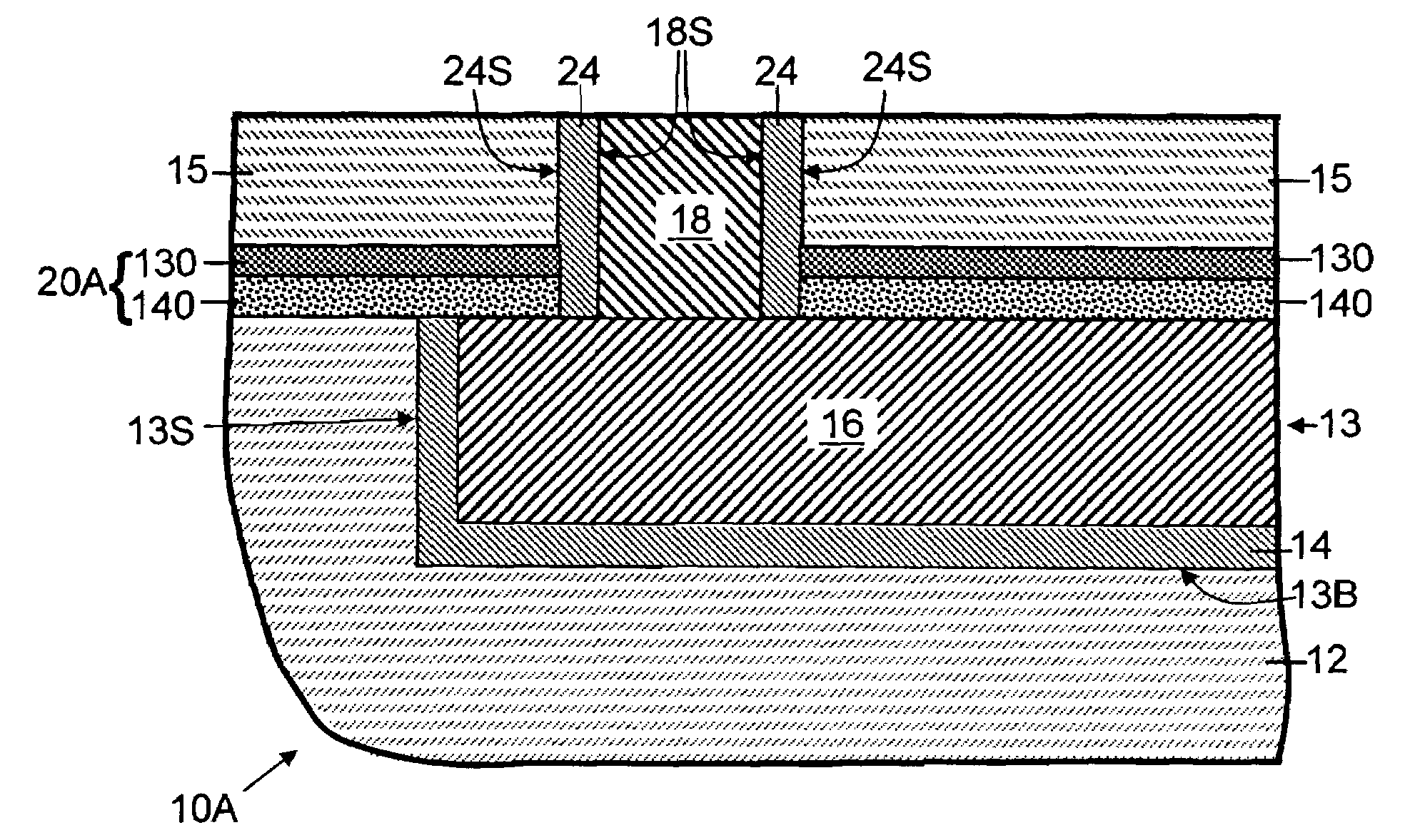
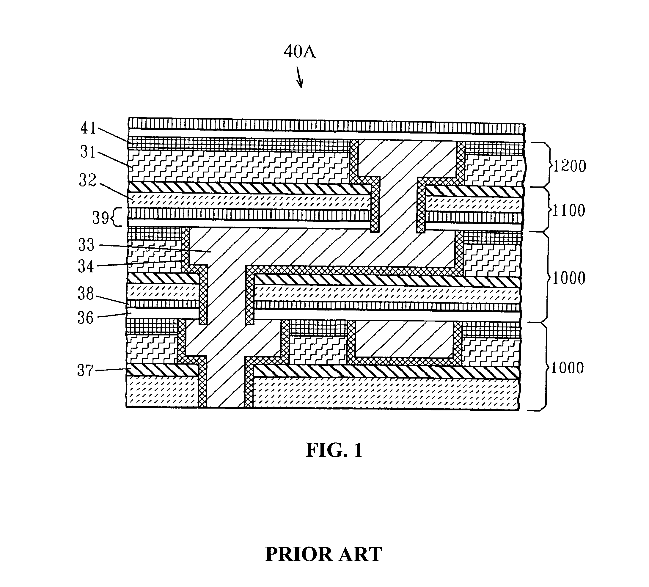
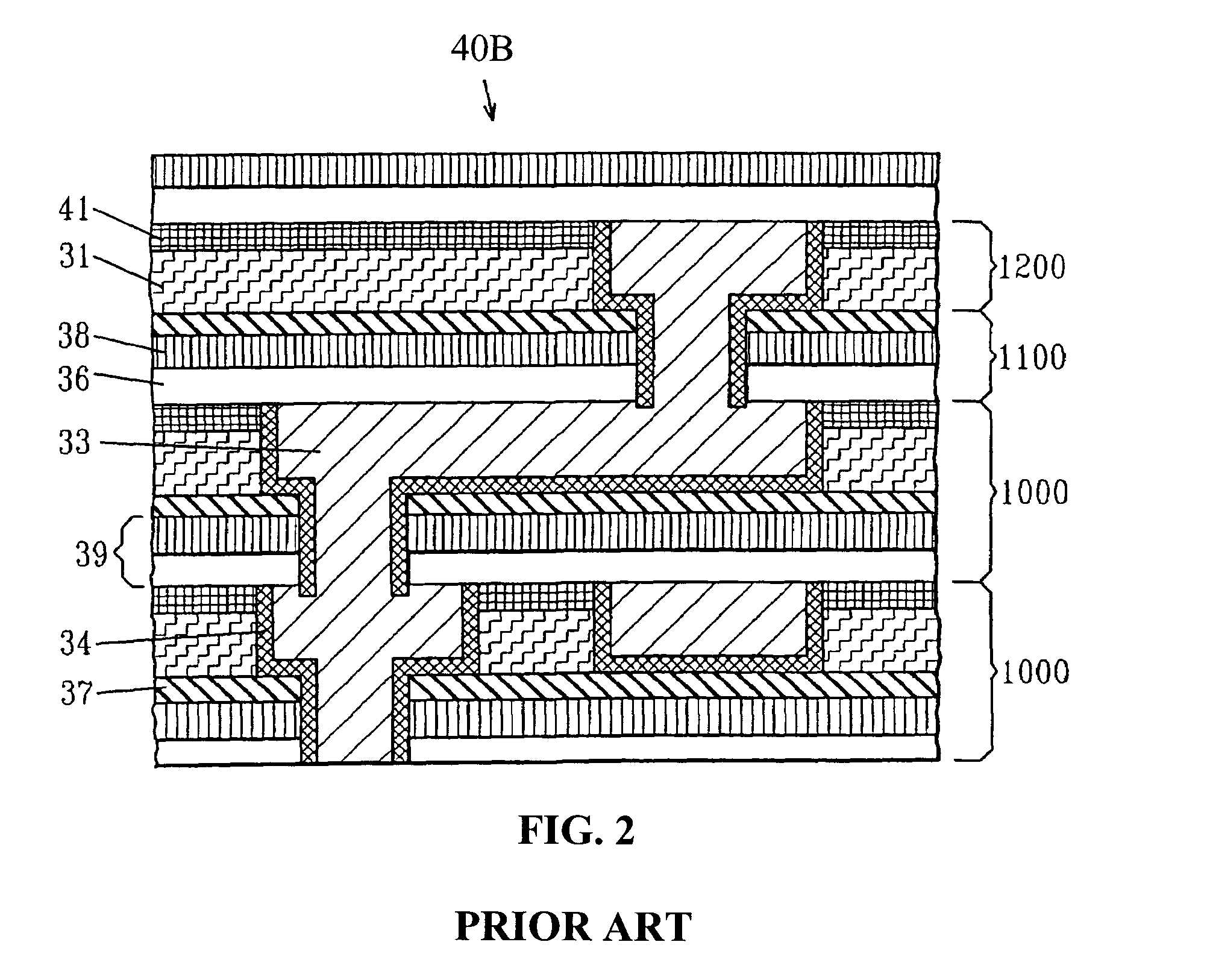
[0059]In one embodiment of the present invention, a multilayered diffusion barrier layer is thermally stable above 300° C., has a thickness between 10 nm and 50 nm, and is comprised of at least two laminated films, i.e. a dual film (bilayer), where at least one film is an air and metal diffusion barrier and at least another of the dual films is a UV blocking film. The multi-film diffusion barrier layer of the present invention may have a variety of configurations including, for example, dual films with the UV blocking film atop the laminated cap barrier, dual films with the cap barrier film atop the UV blocking film, or a triple film (three laminated films or which may be referred to as a trilayer) with the UV blocking film placed between two cap barrier films. For example, (a) if the objective is to prevent UV penetration, the UV blocking film is deposited on top; (b) if the objective is to allow partial UV penetration, the film is inserted in middle of a triple film; and (c) if th...


PUM

PropertyMeasurementUnit
dielectric constantaaaaaaaaaa

Abstract

An interconnect in provided which comprises a copper conductor having both a top surface and a lower surface, with caps formed on the top surface of the metallic conductor. The cap is formed of dual laminations or multiple laminations of films with the laminated films including an Ultra-Violet (UV) blocking film and a diffusion barrier film. The diffusion barrier film and the UV blocking film may be separated by an intermediate film.

Description

BACKGROUND OF THE INVENTION[0001]The present invention relates to protection of the interconnection structures, known as interconnects, in Ultra-Large Scale Integrated (ULSI) microelectronic circuits including high speed microprocessors, application specific integrated circuits, memory storage devices, and related electronic structures with a multilayered barrier layer. More particularly this invention relates to the structure of cap layers for protecting interconnect-metallization in Back End Of Line (BEOL) structures in such ULSI microelectronic circuits.[0002]In traditional semiconductor devices, aluminum and aluminum alloys have been used as interconnect metallurgies for providing electrical connections to and from devices in BEOL layers of the devices. While aluminum-based metallurgies have been the material of choice for use as metal interconnects in the past, aluminum no longer satisfies requirements as circuit density and speeds for semiconductor devices increase and the sca...

Claims


Application Information

Patent Timeline
Patent Type & Authority Applications(United States)
IPC IPC(8): H01L23/532H01L21/768
CPCH01L21/76825H01L21/76832H01L21/76834H01L21/76844H01L2924/0002H01L23/53295H01L2924/00
Inventor BONILLA, GRISELDADIMITRAKOPOULOS, CHRISTOS D.NGUYEN, SON V.GRILL, ALFREDNITTA, SATYANARAYANA V.RESTAINO, DARRYL D.SPOONER, TERRY A.
Owner GLOBALFOUNDRIES INC
Why Eureka
Try Eureka