Semiconductor integrated circuit and power-supply control method

a technology of integrated circuit and power supply, applied in logic circuits, electronic switching, pulse techniques, etc., can solve the problem of long time for technology to execute control, and achieve the effect of reducing the length of time, and gradually shortening the time interval of switch turning on

Inactive Publication Date: 2009-07-16
SONY CORP
View PDF7 Cites 25 Cited by
  • Summary
  • Abstract
  • Description
  • Claims
  • Application Information

AI Technical Summary

Benefits of technology

[0031]Typically, the larger the difference in voltage between the first and second voltage lines in initial switch conduction control, the longer the switch turning-on time interval between a switch conduction control operation carried out to put a switch transistor in a turned-on state and a next switch conduction control operation carried out to put another switch transistor in a turned-on state. That is to say, the switch conduction control section controls a transition of each of the switch transistors from a non-conducting state to a conducting state by turning on the switch transistors at a plurality of switch turning-on time intervals so that, in the course of the entire switch conduction control, the switch turning-on time interval is gradually shortened.
[0032]In either of the embodiments, in initial conduction control for a large difference in voltage between the first and second voltage lines, some of switch transistors are each controlled to enter a conducting state so that the resistance between the first and second voltage lines does not abruptly decrease. Thus, the maximum magnitude of a current flowing through the first voltage line is small. As a result, it is possib

Problems solved by technology

In accordance with the technology disclosed in non-patent document 1, however, even though the pea

Method used


Image

  • Semiconductor integrated circuit and power-supply control method
  • Semiconductor integrated circuit and power-supply control method
  • Semiconductor integrated circuit and power-supply control method

Examples


Embodiment Construction

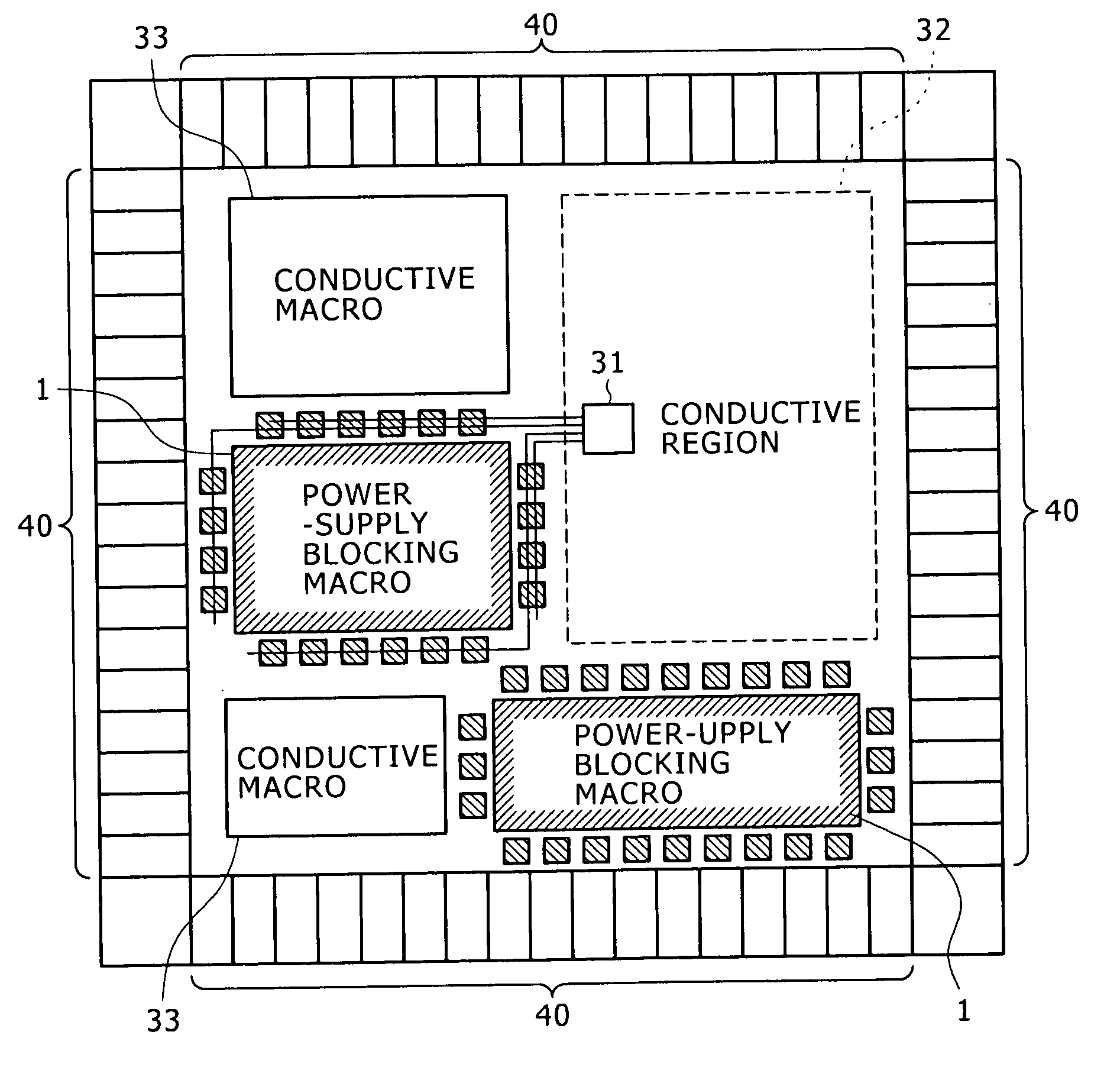
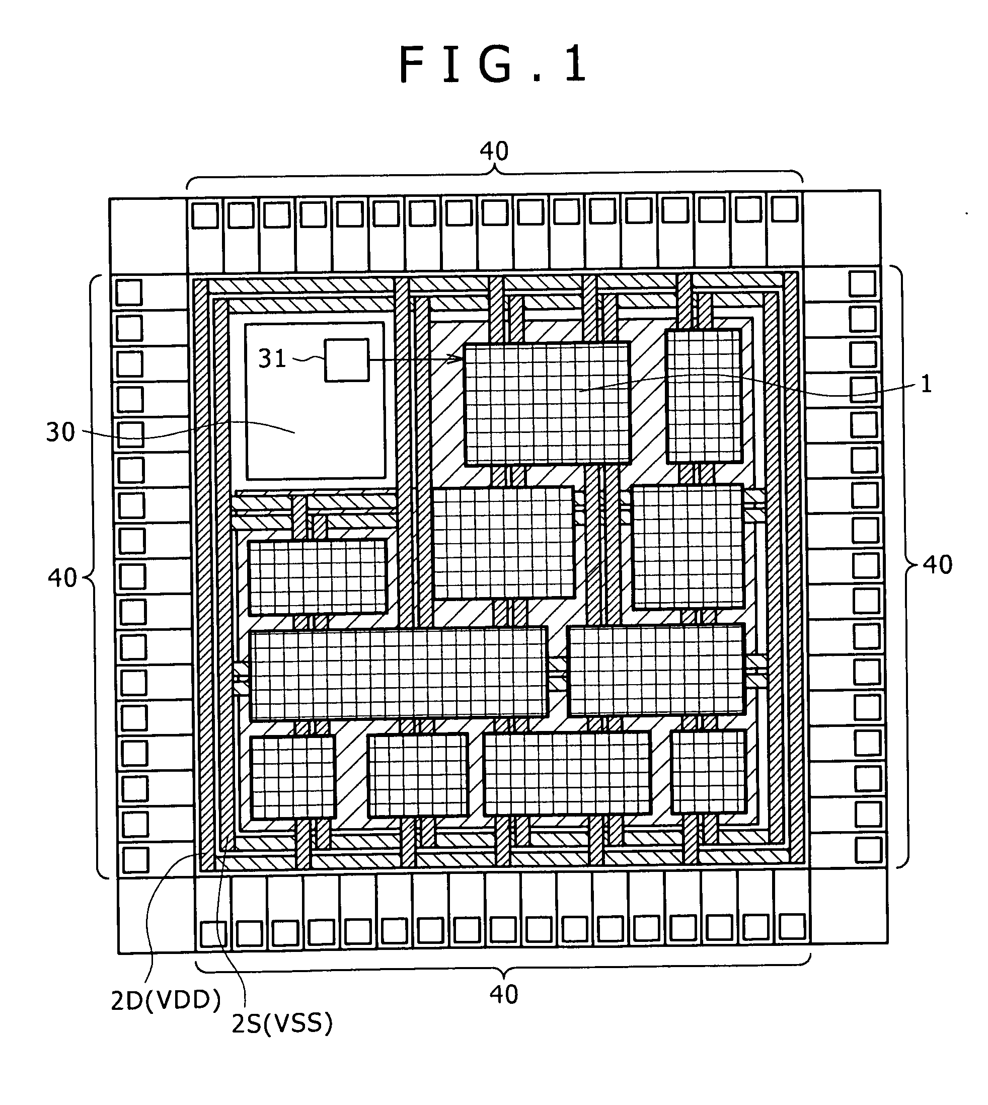
[0046]FIG. 1 is a block diagram showing a first typical overall configuration of a semiconductor integrated circuit according to an embodiment of the present invention.

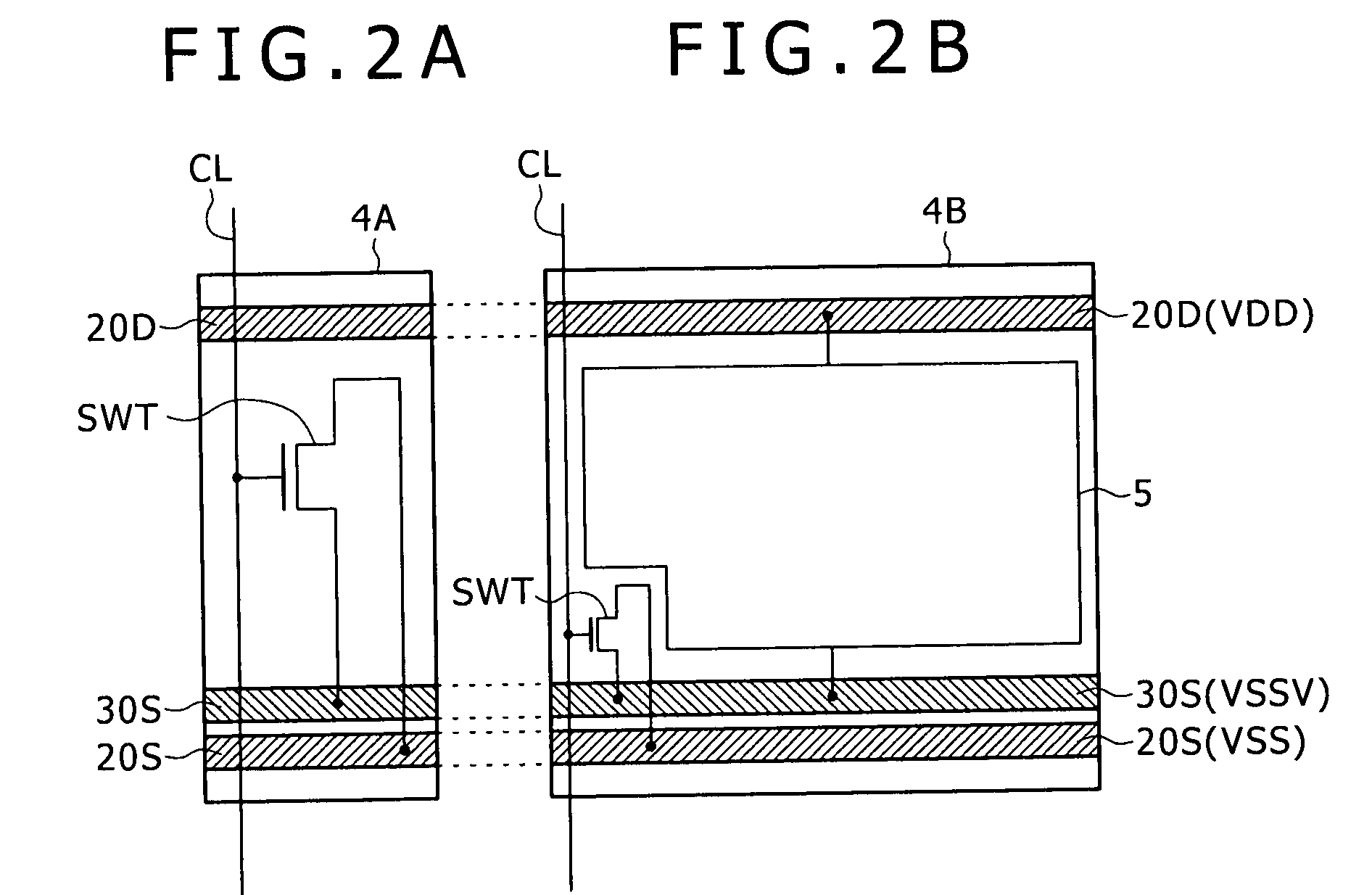
[0047]In the configuration shown in FIG. 1, a plurality of input / output cells 40 are arranged to form an array along each of the four sides of a rectangular semiconductor chip in which the semiconductor integrated circuit is created. In a chip area surrounded by the input / output cells 40, a real VDD line 2D and a real VSS line 2S are provided as first voltage lines. To put it in detail, the real-voltage line pairs (2D, 2S) are oriented in the horizontal (row) direction and the vertical (column) direction so as to form a voltage line layout having the shape of a lattice. In addition, the real-voltage line pairs (2D, 2S) surround each lattice square, forming the external lattice frame of the lattice square. The external lattice frame of a lattice square serves as a number of power-supply points for the lattice square.

[0...


PUM


Abstract

A semiconductor integrated circuit includes: a first voltage line on which a specific one of a power-supply voltage and a reference voltage appears; a second voltage line; a plurality of circuit cells each receiving power generated as a difference between a voltage appearing on the second voltage line and the other one of the power-supply voltage and the reference voltage; a plurality of switch transistors connected in parallel between the first and second voltage lines to serve as switch transistors including switch transistors each having different conducting-state resistances; and a switch conduction control section for controlling a transition of each of the switch transistors from a non-conducting state to a conducting state by turning on the switch transistors at separate points of time.

Description

CROSS REFERENCES TO RELATED APPLICATIONS[0001]The present invention contains subject matter related Japanese Patent Application JP 2008-006955 filed in the Japan Patent Office on Jan. 16, 2008, the entire contents of which being incorporated herein by reference.BACKGROUND OF THE INVENTION[0002]1. Field of the Invention[0003]The present invention relates to a semiconductor integrated circuit for controlling a transition of a plurality of switch transistors, which are used for supplying power to a plurality of circuit cells and cutting off the supply of power to the circuit cells, from a turned-off state to a turned-on state and relates to a power-supply control method for controlling such a transition.[0004]2. Description of the Related Art[0005]A MTCMOS (Multi-threshold Complementary Metal Oxide Semiconductor) technology is known as a technology for controlling switch transistors, which are used for supplying power to a circuit and cutting of the supply of power to the circuit.[0006...

Claims


Application Information

Patent Timeline
IPC IPC(8): H03K17/687
CPCH03K17/102H03K19/0016H03K17/164
Inventor IGARASHI, MASAHIROMOTOMURA, TETSUOKANEKO, RYUJIFUJIWARA, MAKOTOTANAKA, YOSHINORIOGATA, HIROMI
Owner SONY CORP
Why Eureka
Try Eureka