Resistance change type memory
a type memory and resistance change technology, applied in the field of resistance change type memory, can solve the problems of affecting reading sensitivity, affecting retention, and disassembly and maintenance,
- Summary
- Abstract
- Description
- Claims
- Application Information
AI Technical Summary
Benefits of technology
Problems solved by technology
Method used
Image
Examples
first embodiment
(1) First Embodiment
[0141]A. Circuit Arrangement (First Example)
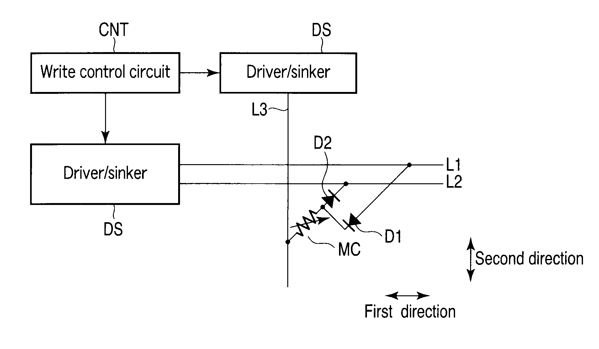
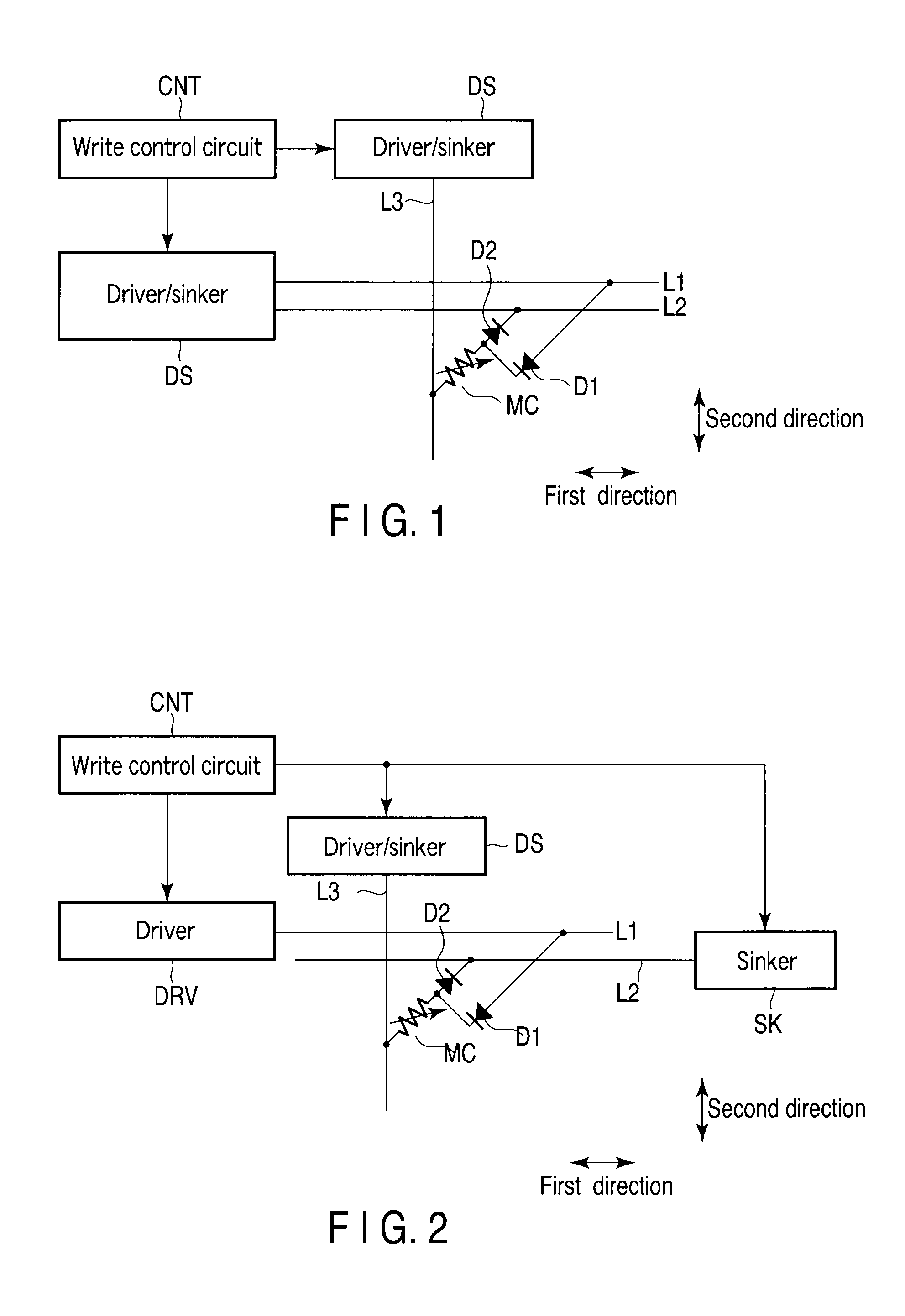
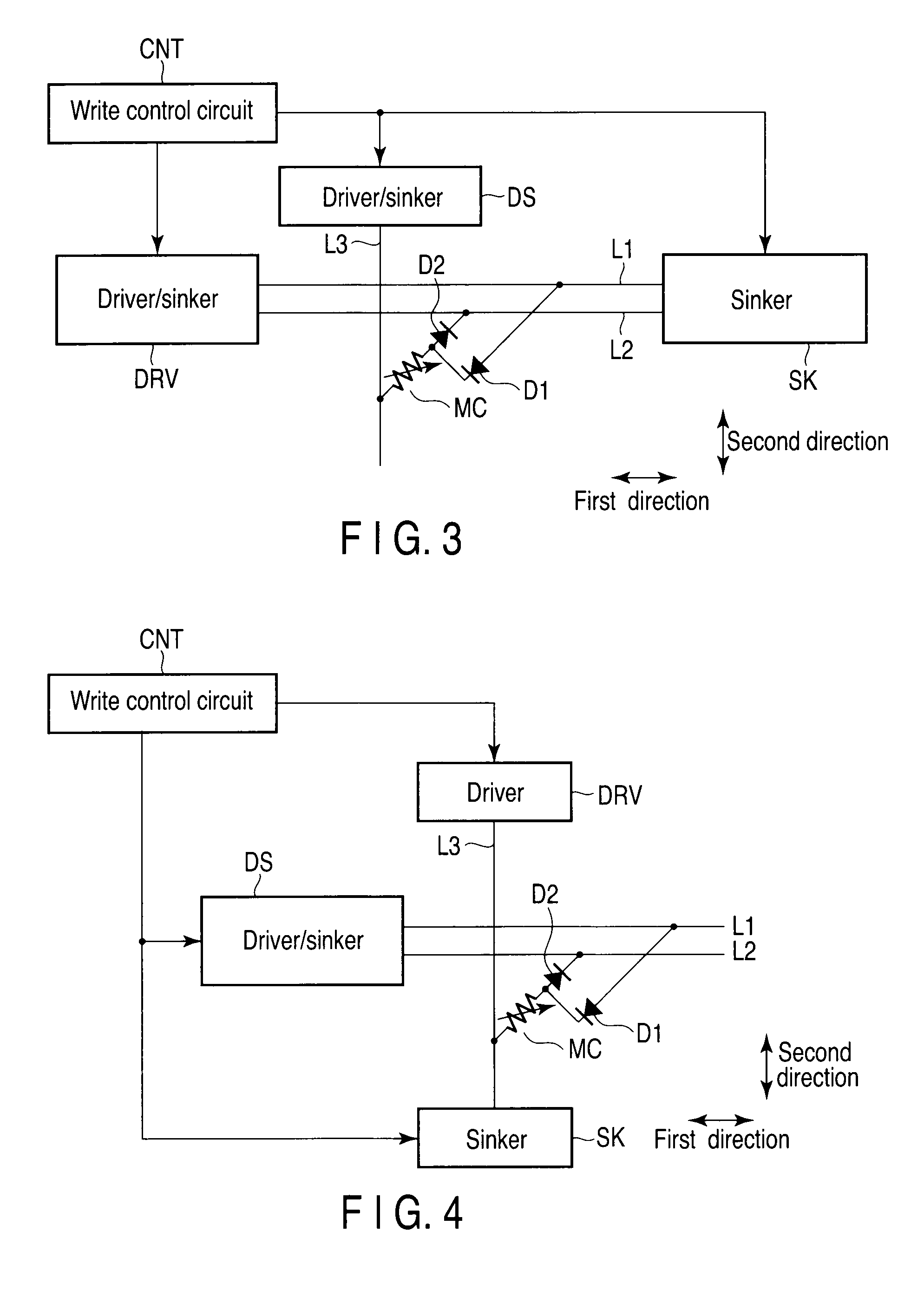
[0142]The circuit shows a specific arrangement of the second basic architecture (FIG. 2).
[0143]FIGS. 9 to 11 show a write circuit of the resistance change type memory of the present invention.
[0144]A memory cell array 11 is composed of a plurality of memory cells. Four memory cells MC1, MC2, MC3, MC4 are shown here for simplification.
[0145]The memory cells MC1, MC2, MC3, MC4 are resistance change elements.
[0146]Word lines WL1a, WL1b, WL2a, WL2b, which extend in a first direction, are disposed on the memory cell array 11. The word lines WL1a, WL1b constitute a word line pair and are disposed in correspondence to the memory cells MC1, MC3. Likewise, the word lines WL2a, WL2b constitute a word line pair and are disposed in correspondence to the memory cells MC2, MC4.
[0147]One ends of the word lines WL1a, WL2a are connected to a word line driver 13 through a word line selector 12. One ends of the word lines WL1b, WL2b are p...
third example
[0233]FIG. 22 shows a third example of the device structure.
[0234]Diodes D1a, D1b of the third example have a structure different from that of the first example. The other arrangements of the third example are the same as those of the first example.
[0235]N-well regions 35a, 35b are formed in an element region surrounded by an element separation insulation layer 22.
[0236]A diode D1a composed of an n+ diffusion layer 36a and a p+ diffusion layer 37a is formed in the n-well region 35a. Further, a diode D1b composed of an n+ diffusion layer 36b and a p+ diffusion layer 37b is formed in the n-well region 35b.
[0237]The p+ diffusion layer 37a as an anode of the diode D1a is connected to a word line WL1a through a plug 25, and the n+ diffusion layer 36a thereof as a cathode is connected to an intermediate conductive layer 29 through a plug 27.
[0238]The p+ diffusion layer 37b as an anode of the diode D1b is connected to the intermediate conductive layer 29 through the plug 28, and the n+ di...
fourth example
[0240]FIG. 23 shows a fourth example of the device structure.
[0241]The device structure of the fourth example is constructed by combining the device structures of the second and third examples.
[0242]Diodes D1a, D1b are formed on an SOI substrate.
[0243]The diode D1a is composed of an n+ diffusion layer 36a and a p+ diffusion layer 37a in an n-well region 35a. The diode D1b composed of an n+ diffusion layer 36b and a p+ diffusion layer 37b in an n-well region 35b.
[0244]Since diffusion of impurities can be suppressed by using the SOI substrate, the distance between the diodes D1a, D1b can be reduced while sufficiently securing an element separation function.
PUM
 Abstract
Description
Claims
Application Information


