Method to extract gate to source/drain and overlap capacitances and test key structure therefor

a technology of overlap capacitance and gate to source/drain, which is applied in the direction of individual semiconductor device testing, semiconductor/solid-state device testing/measurement, instruments, etc., can solve the problems of parasitic capacitance effects becoming noticeable and/or problemati

Active Publication Date: 2009-07-23
UNITED MICROELECTRONICS CORP
View PDF6 Cites 33 Cited by
  • Summary
  • Abstract
  • Description
  • Claims
  • Application Information

AI Technical Summary

Problems solved by technology

As device sizes continue to shrink, however, parasitic capacitance effects may become noticeable and / or problematic.

Method used


Image

  • Method to extract gate to source/drain and overlap capacitances and test key structure therefor
  • Method to extract gate to source/drain and overlap capacitances and test key structure therefor
  • Method to extract gate to source/drain and overlap capacitances and test key structure therefor

Examples


Embodiment Construction

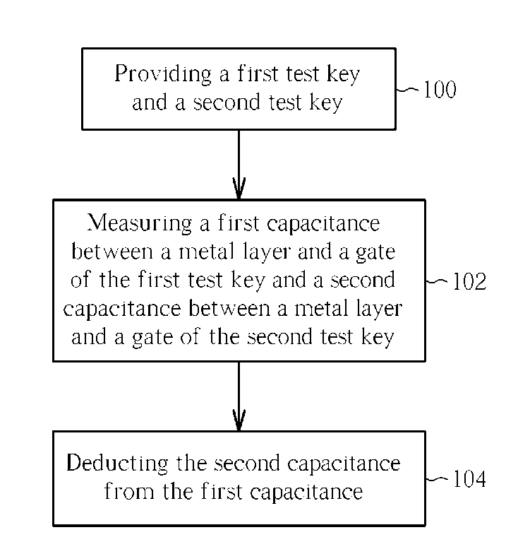
[0027]In order to obtain a pure gate to source / drain and overlap capacitances, the method according to the present invention is characterized that, by utilizing a test key having a novel structure and a reference test key, the gate to source / drain and overlap capacitances can be decoupled.

[0028]FIG. 2 illustrates the steps of the method of the present invention. In Step 100, a first test key and a second test key are provided. In Step 102, a first capacitance between a metal layer and a gate of the first test key and a second capacitance between a metal layer and a gate of the second test key are measured. In Step 104, the second capacitance is deducted from the first capacitance, thereby to obtain a resultant capacitance.

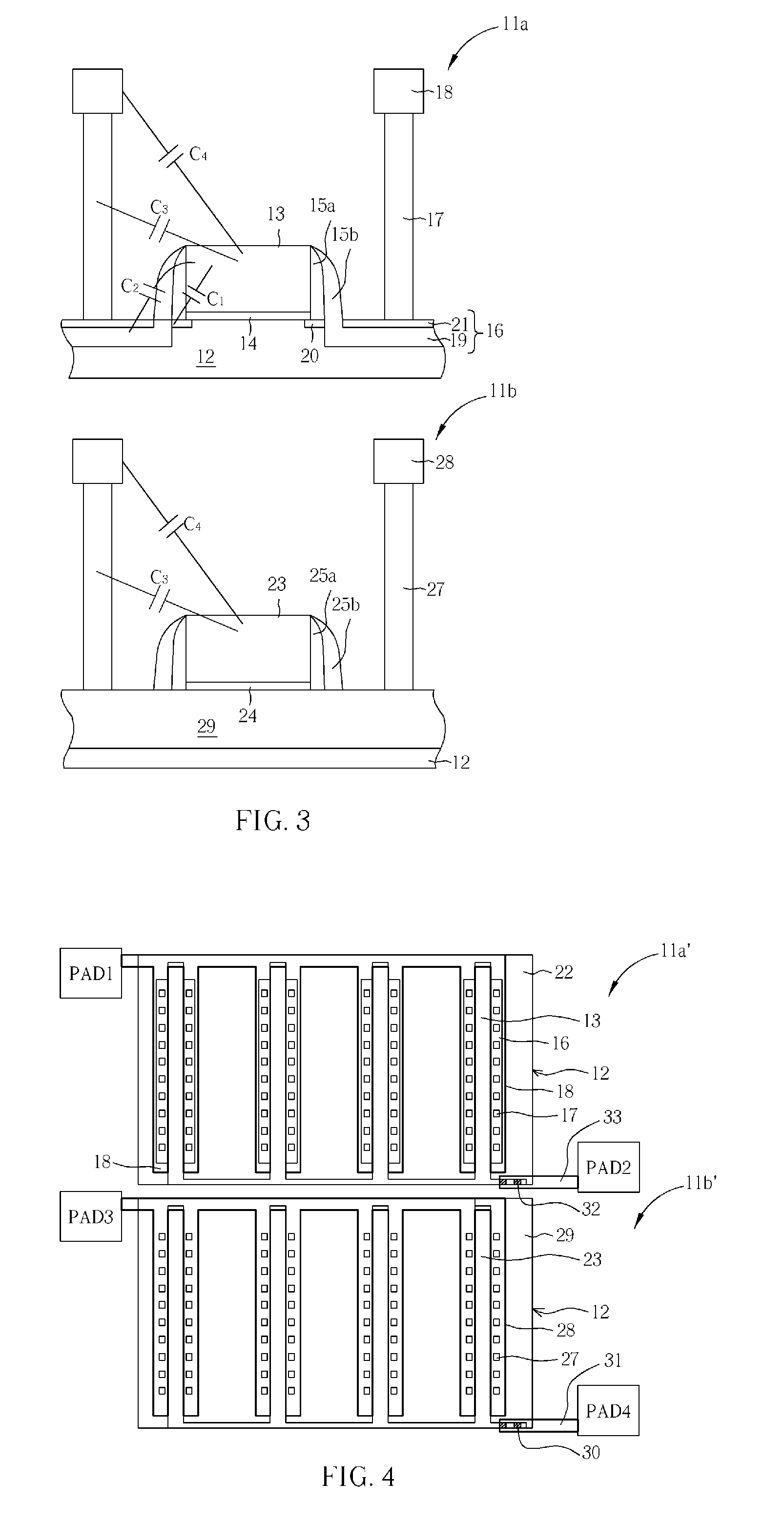
[0029]The first test key comprises at least a first gate, at least a first gate dielectric layer, at least a first spacer, at least a first doping region, at least a first contact and a first metal layer. The second test key comprises at least a second gate, at lea...


PUM


Abstract

A method to extract gate to source / drain and overlap capacitances is disclosed. A first capacitance of a first test key having a reference structure and a second capacitance of a second test key having a novel structure are measured. The second test key may comprise at least a gate formed on an insulation structure, at least a contact formed on the insulation structure aside, and a metal layer formed on the contact. Another embodiment of the second test key may comprise at least a gate formed on the semiconductor substrate, a contact formed aside, and a metal layer formed on the contact. Further another embodiment uses a test key comprising at least an elongated gate and an elongated doping region aside, and only one or a few contacts are formed on an end portion of the elongated doping region.

Description

BACKGROUND OF THE INVENTION[0001]1. Field of the Invention[0002]The present invention relates to decoupling gate to contact and gate to metal capacitances from overall gate capacitance, and particularly to a method to extract gate to source / drain and overlap capacitances and a test key structure used for the method.[0003]2. Description of the Prior Art[0004]In the semiconductor industry there is a continuing trend toward manufacturing integrated circuits (ICs) with higher densities. Accordingly, smaller feature sizes, smaller separations between features and more precise feature shapes are required in integrated circuits (ICs) fabricated on small rectangular portions of the wafer, commonly known as dies. This may include the width and spacing of interconnecting lines, spacing and diameter of contact holes, as well as the surface geometry of various other features (e.g., corners and edges). The scaling-down of integrated circuit dimensions can facilitate faster circuit performance an...

Claims


Application Information

Patent Timeline
Patent Type & Authority Applications(United States)
IPC IPC(8): H01L21/66
CPCH01L22/34H01L22/14
Inventor HSU, YU-HAOYEH, KUO-LIANG
Owner UNITED MICROELECTRONICS CORP
Why Eureka
Try Eureka