
Eureka
For R&D, Eureka makes reading and utilizing patents & technical documents easy.
Eureka AIR
Designed for self-driven R&D workflows. Generate viable solutions, solve complex R&D challenges, empower your innovation with AI.

Eureka Materials
Designed for material experts only. Revolutionize your material R&D, from search, analyze, to developing new materials.

TechResearch
Generate reliable direction feasibility study reports for your R&D in just a few steps.

TechSeek
Discover and master advanced knowledge NOW. Basics, ideas, possibilities, all at once.

TechMind
As an expert in R&D Theories, TechMind can generates customized viable solutions instantly.

TechRisk
Analyze your overall solution with one click, know your potential R&D risks in advance.

TechMonitor
Get weekly tech updates, stay abreast of the latest tech innovations and key insights.
Switch circuit
- Summary
- Abstract
- Description
- Claims
- Application Information
AI Technical Summary
Benefits of technology
Problems solved by technology
Method used
Image

Examples
first exemplary embodiment
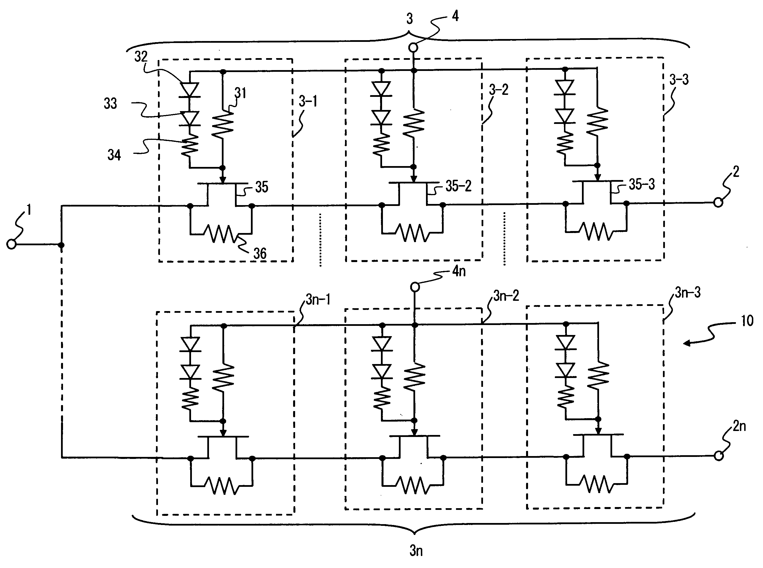
[0025]FIG. 1 is a circuit diagram showing a switch circuit 10 in accordance with an exemplary embodiment of the present invention. As shown in FIG. 1, the switch circuit 10 for a high frequency in accordance with an exemplary embodiment includes input / output terminal 1 (which is hereinafter explained mainly as to function as an input terminal to distinguish from input / output terminals 2), a plurality of input / output terminals 2-2n (which are hereinafter explained mainly as to function as output terminals to distinguish from the input / output terminal 1), a plurality of switch elements 3-3n, and a plurality of control terminals 4-4n. That is, the switch circuit 10 in accordance with an exemplary embodiment is a SPnT switch. The switch circuit 10 is, for example, a switch circuit to make a “1-to-n” connection for a single antenna.
[0026]Note that the switch circuit 10 shown in FIG. 1 is a switch circuit to input and output a signal in a high frequency band such as a frequency band in th...
second exemplary embodiment
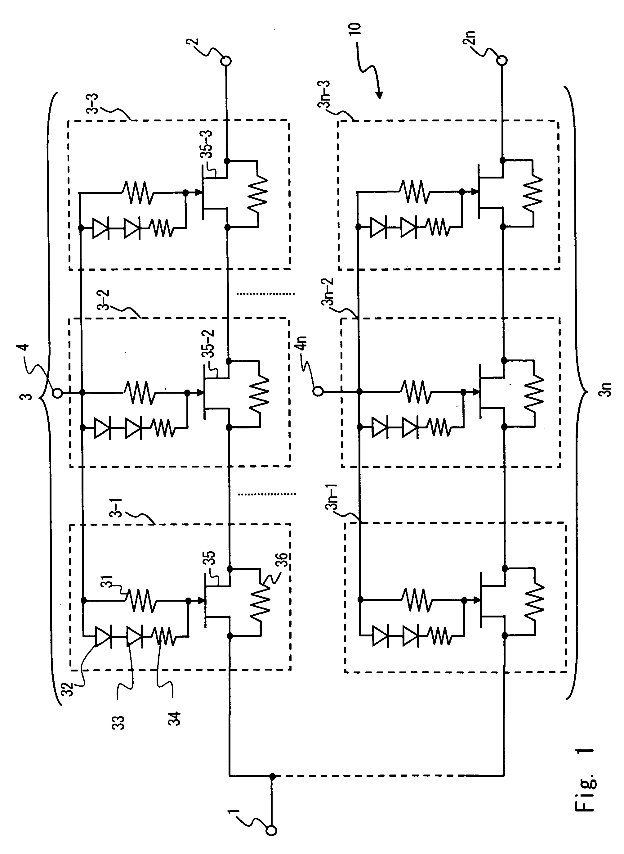
[0043]In the previous exemplary embodiment, a switch circuit, in which a signal provided to the control terminal 4 is changed from a low level to a high level, is explained. In an exemplary embodiment described hereinafter, a switch circuit 20 in accordance with another exemplary embodiment of the present invention, in which a signal provided to the control terminal 4 is changed from a high level to a low level, is explained. FIG. 5 is a circuit diagram showing a switch circuit 20 in accordance with another exemplary embodiment of the present invention. The structures other than the structures within the switch circuits 3 shown in FIG. 1 are the same as those in the previous exemplary embodiment. Therefore, the same signs are assigned to the same components, and explanation of them is omitted. The switch circuit 20 in accordance with this exemplary embodiment of the present invention is different from the previous exemplary embodiment in the switch elements 23. In particular, the st...
first modified example
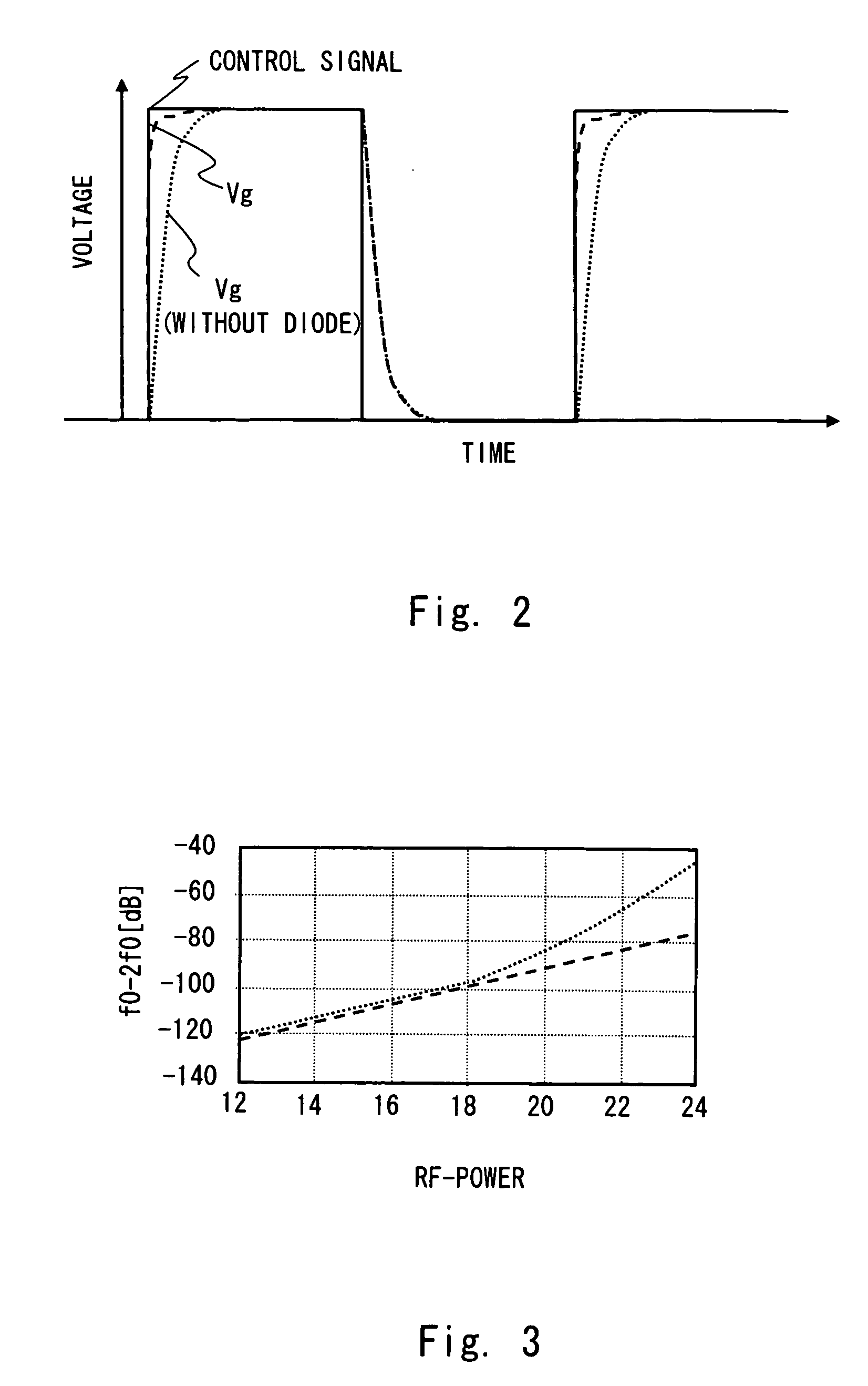
[0049]FIG. 7 is a circuit diagram showing a modified example of the previous exemplary embodiments. This modified example is formed by combining the switch circuits 10 and 20 explained in the previous exemplary embodiments. Therefore, the same signs are assigned to the same components as those of the previous exemplary embodiments, and explanation of them is omitted. By forming a circuit as shown in FIG. 7, it is possible to make the conductive state of the J-FET follow the changes at high speed regardless of whether the control signal is changed from the low level to the high level or from the high level to the low level. FIG. 8 shows changes in agate potential with respect to changes in a control signal in the switch circuit shown in FIG. 7. Similarly to FIGS. 2 and 6, the solid line represents changes in the control signal input to the control terminal 4. The broken line represents changes in the gate potential Vg in an exemplary embodiment. Furthermore, the dotted line represent...
PUM
 Abstract
Description
Claims
Application Information
 - R&D Engineer
- R&D Manager
- IP Professional
- Industry Leading Data Capabilities
- Powerful AI technology
- Patent DNA Extraction
Browse by: Latest US Patents, China's latest patents, Technical Efficacy Thesaurus, Application Domain, Technology Topic, Popular Technical Reports.
© 2024 PatSnap. All rights reserved.Legal|Privacy policy|Modern Slavery Act Transparency Statement|Sitemap|About US| Contact US: help@patsnap.com