Fabrication of advanced thermoelectric materials by hierarchical nanovoid generation

a nano-void and thermoelectric material technology, applied in the field of thermoelectric materials, can solve the problems of poor void fraction performance of most test samples with a certain void fraction, limited system design and application, and poor void fraction performance of te devices, including te generators or te coolers

Inactive Publication Date: 2009-07-23
NASA +1
View PDF7 Cites 17 Cited by
  • Summary
  • Abstract
  • Description
  • Claims
  • Application Information

AI Technical Summary

Problems solved by technology

Many TE materials have been brought into laboratory tests but the overall findings are less than impressive.
Previously, poor TE properties of TE devices, including TE generators or TE coolers, have limited system design and application.
Nevertheless, most test samples with a certain void fraction have shown unsatisfactory performance due to failure in design and failure to synthesize proper nanovoid structure.
In this regard, material design and synthesis are critical to achieving this goal since nature does not allow these two properties at the same time.
Organic groups grafted to metal precursors are unstable and removed easily during heating process.
In the previous attempts to develop TE materials having a void structure, most of the void structures are poorly defined in terms of void size and interconnectivity.
Conventional fabrication techniques don't allow a sophisticated control of nanoscale structure.
Most void structures form interconnected void channels which disturb electron mobility and cause electrical failure.

Method used


Image

  • Fabrication of advanced thermoelectric materials by hierarchical nanovoid generation
  • Fabrication of advanced thermoelectric materials by hierarchical nanovoid generation
  • Fabrication of advanced thermoelectric materials by hierarchical nanovoid generation

Examples


Embodiment Construction

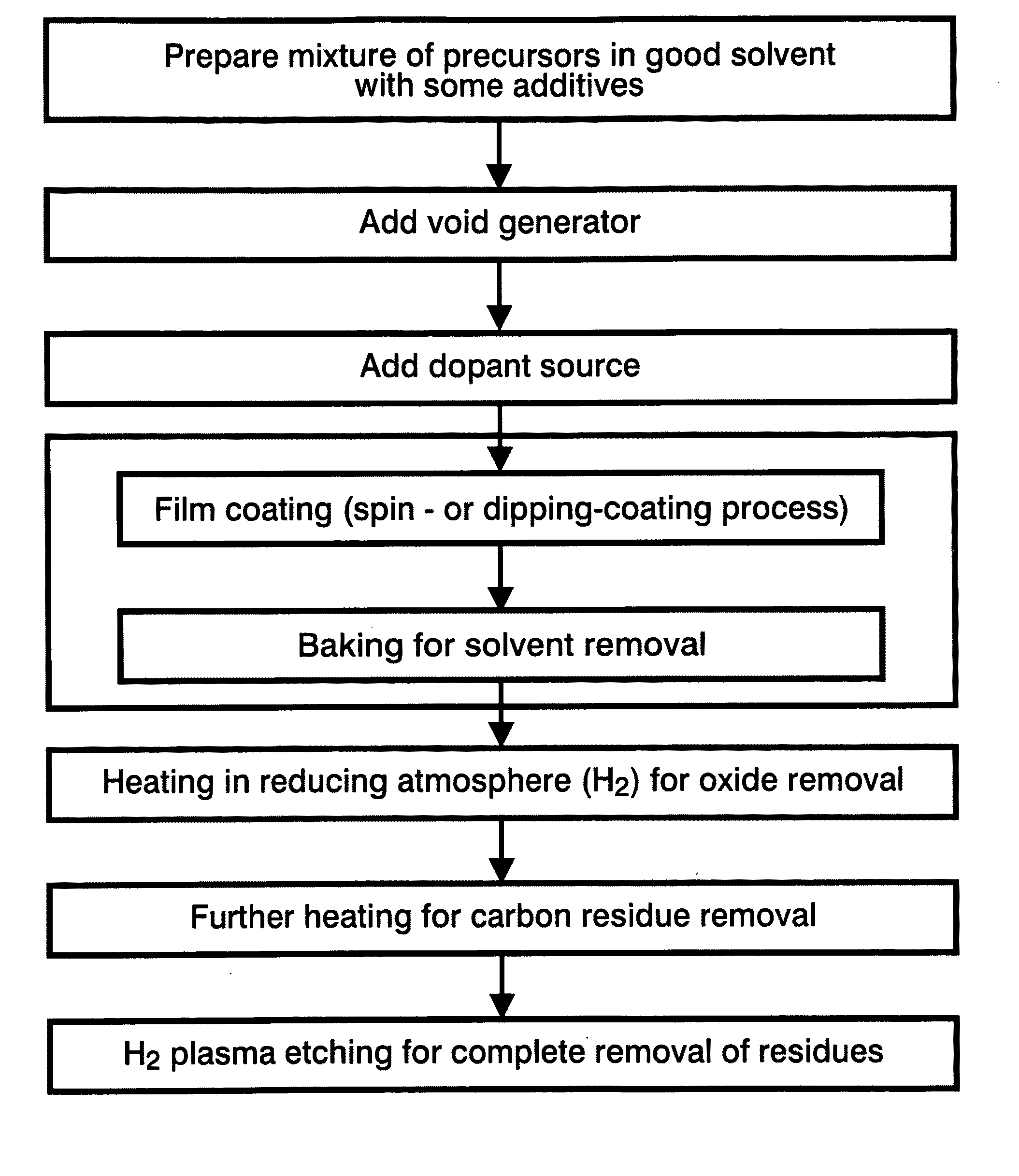
[0029]The following detailed description is of the best presently contemplated mode of carrying out the invention. This description is not to be taken in a limiting sense, but is made merely for the purpose of illustrating general principles of embodiments of the invention.

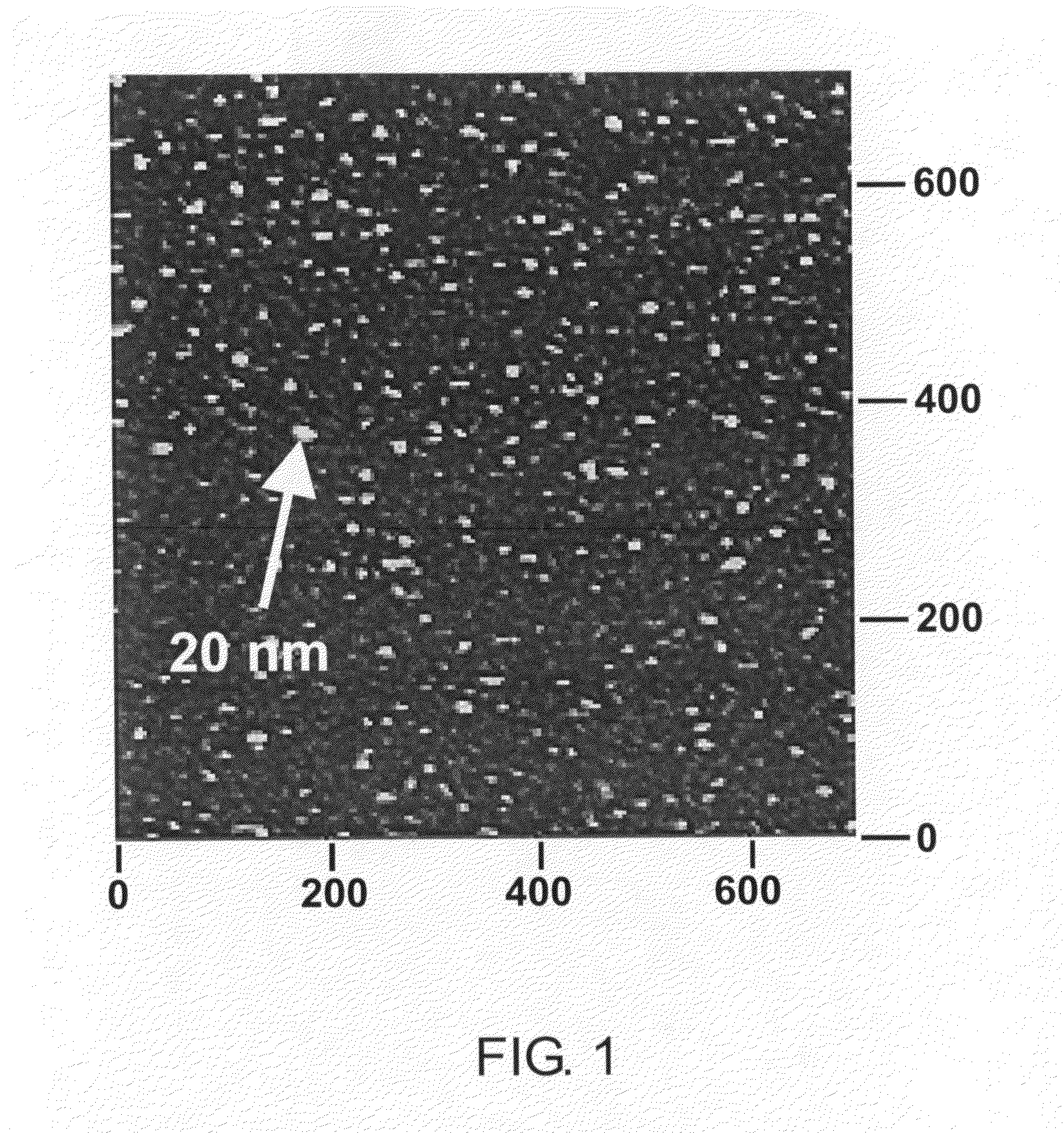
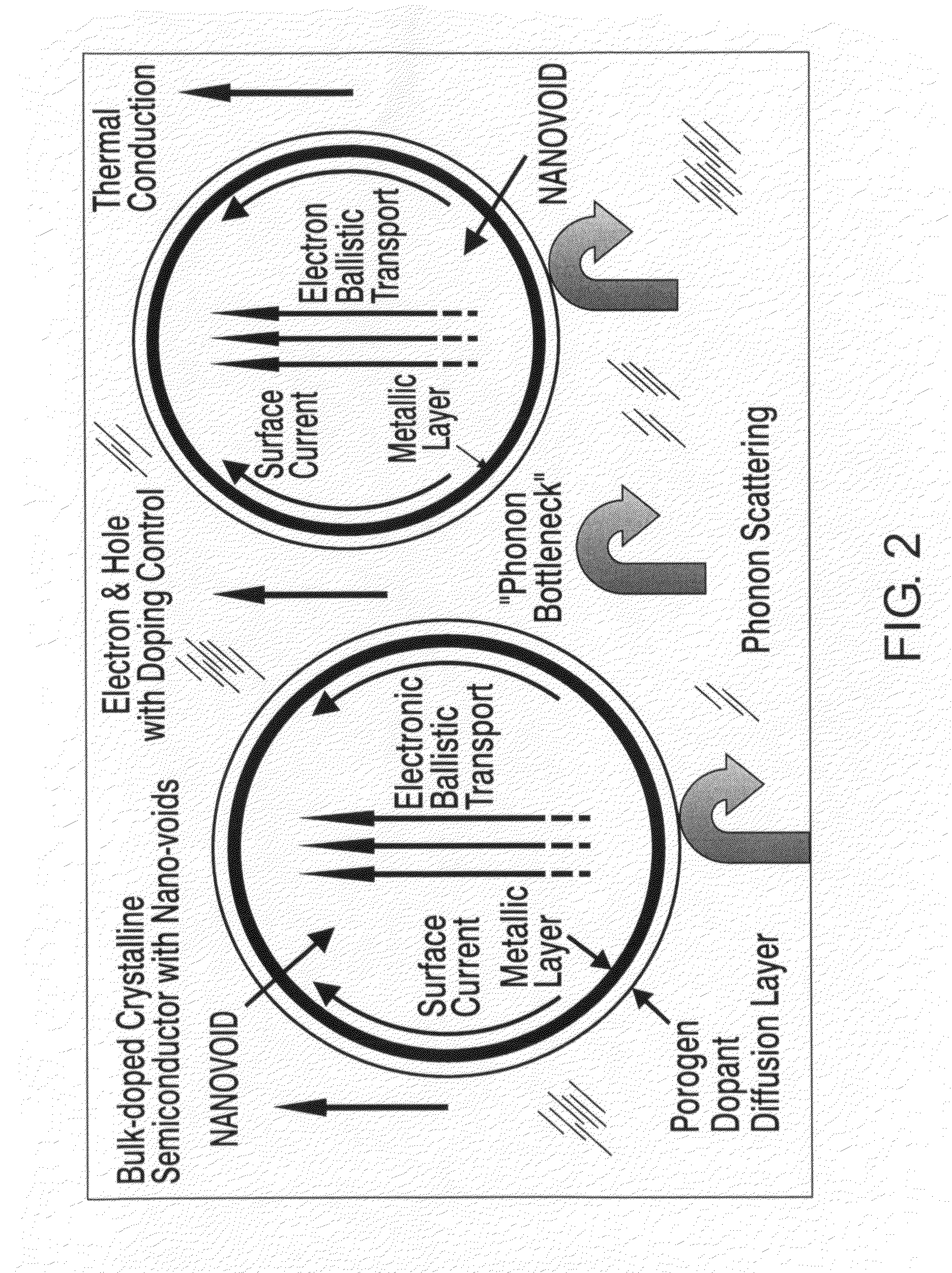
[0030]The new technology presented here is based on the structural modification of TE materials by imbedding nanovoids to increase electrical conductivity and to decrease thermal conductivity to achieve ZT values greater than 5.0. The current invention teaches that the nanovoids imbedded within semiconductor materials enhance the electrical conductivity. Additionally, the electrical conductivity increases with the increasing fraction of nanovoids that were created by a porosity generator (“porogen”). This is a startling result. The inventors strongly believe that this result is the indication of electrons' ballistic behavior within a nanovoid under the wave-particle duality condition. On the other hand, the phonon...


PUM

PropertyMeasurementUnit
diametersaaaaaaaaaa
thermoelectricaaaaaaaaaa
thicknessaaaaaaaaaa

Abstract

A novel method to prepare an advanced thermoelectric material has hierarchical structures embedded with nanometer-sized voids which are key to enhancement of the thermoelectric performance. Solution-based thin film deposition technique enables preparation of stable film of thermoelectric material and void generator (voigen). A subsequent thermal process creates hierarchical nanovoid structure inside the thermoelectric material. Potential application areas of this advanced thermoelectric material with nanovoid structure are commercial applications (electronics cooling), medical and scientific applications (biological analysis device, medical imaging systems), telecommunications, and defense and military applications (night vision equipments).

Description

CROSS REFERENCE TO RELATED APPLICATION[0001]The present application claims priority from U.S. Provisional Application Ser. No. 61 / 005,229, filed Dec. 4, 2007 and U.S. Provisional Application Ser. No. 61 / 005,226, filed Dec. 4, 2007. This application is related to copending U.S. application Ser. No. 11 / 831,233, filed on Jul. 31, 2007 for “Configuration and Power Technology for Application-Specific Scenarios of High Altitude Airships,” U.S. application Ser. No. ______, filed on Nov. 26, 2008 for “Metallized Nanotube Polymer Composite (MNPC) and Methods for Making Same”, U.S. application Ser. No. 11 / 827,567 filed on Jul. 12, 2007 for “Fabrication of Metal Nanoshells,” and U.S. application Ser. No. ______, filed on Dec. 4, 2008 for “Fabrication Of Metallic Hollow Nanoparticles”, all of which are hereby incorporated by reference herein.STATEMENT REGARDING FEDERALLY SPONSORED RESEARCH OR DEVELOPMENT[0002]The U.S. Government has a paid-up license in this invention and the right in limited c...

Claims


Application Information

Patent Timeline
Patent Type & Authority Applications(United States)
IPC IPC(8): B22F1/00
CPCB22F2998/00C22C1/04B22F1/054
Inventor T
Owner NASA
Why Eureka
Try Eureka