Methodology and system for determining numerical errors in pixel-based imaging simulation in designing lithographic masks

a lithographic mask and image simulation technology, applied in the field of very large scale integrated circuit fabrication, can solve the problems of increasing computation costs, inability to compute, and inability to accurately simulate images

Inactive Publication Date: 2009-07-30
GLOBALFOUNDRIES INC
View PDF12 Cites 23 Cited by
  • Summary
  • Abstract
  • Description
  • Claims
  • Application Information

AI Technical Summary

Problems solved by technology

Such edge fragments are typically unevenly spaced.
However, as IC technology drives towards smaller and denser layouts, the computational cost of simulating images is becoming increasingly impractical.
Large values of k can increase the accuracy of interpolation of the image values between computed pixel grid points but significantly add to the cost of computation.
Although dense pixel-based image computation is computationally efficient, some of the steps described in FIG. 3 are inherently prone to a variety of errors due to numerical and discretization.
For example, rasterization (described as 302 in FIG. 3) can result in discretization errors.
The sampling to Nyquist grid (401) can have problems such as under-sampling.
Both FFT (304) and Inverse FFT (307) can have problems such as numerical errors or frequency errors.
However, in designing and calibration of the grid for a pixel-based simulation, it may be difficult to determine whether inaccuracies in a specific grid implementation are due to discretization or numerical errors or errors in the approximations used in the physical representation of the lithographic process.

Method used


Image

  • Methodology and system for determining numerical errors in pixel-based imaging simulation in designing lithographic masks
  • Methodology and system for determining numerical errors in pixel-based imaging simulation in designing lithographic masks
  • Methodology and system for determining numerical errors in pixel-based imaging simulation in designing lithographic masks

Examples


Embodiment Construction

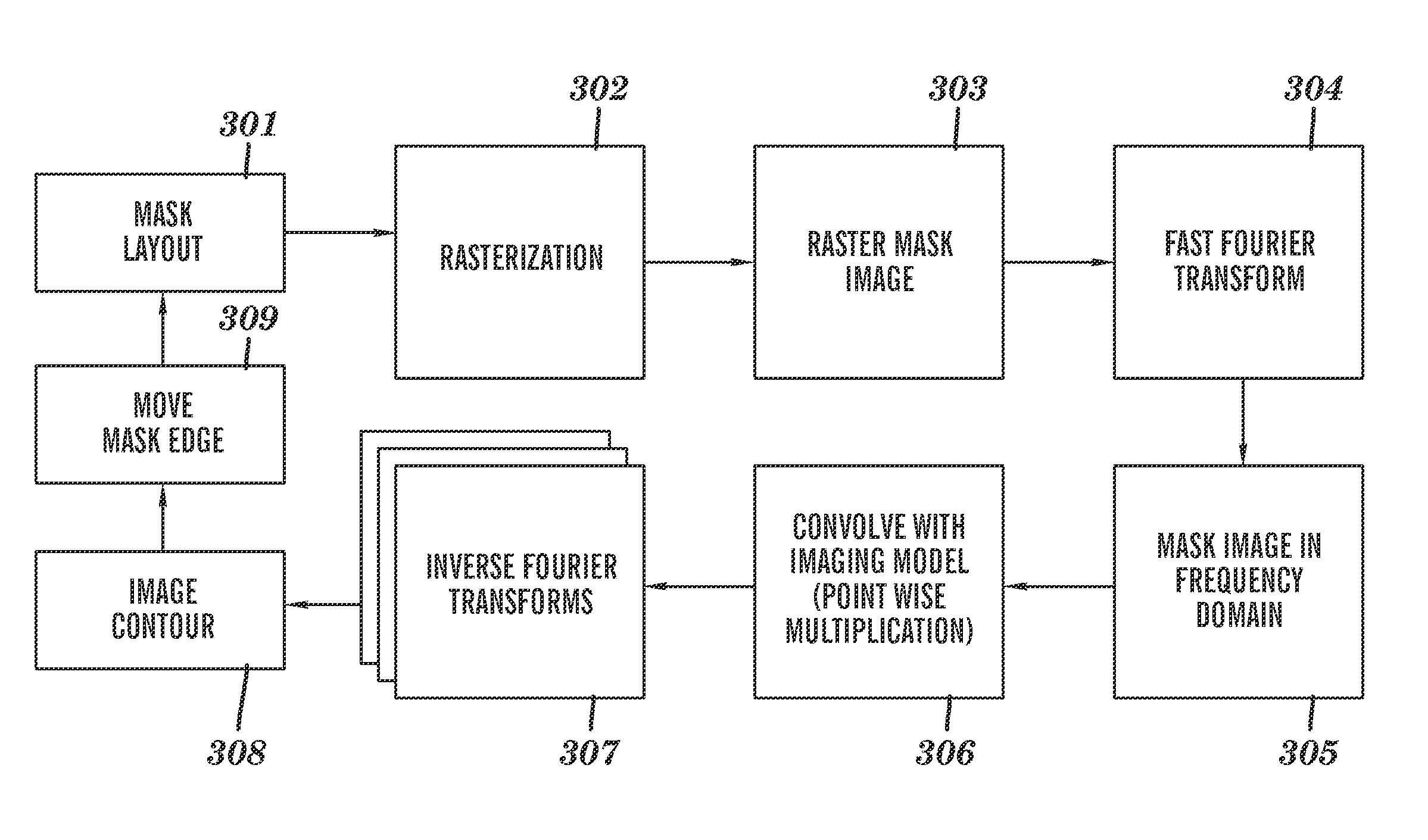
[0045]In accordance with the present invention, test structures are designed to characterize numerical and / or discretization errors in pixel-based process models used in designing lithographic masks. In a pixel-based process model, the pixel grid is typically designed to be uniform along a particular direction. The spacing in the x direction may be different than in the orthogonal y direction, but will be uniform along a given direction.

[0046]The selection of the size of the pixel grid elements is based on the effective resolution of the lithographic process, which is related to the Raleigh limit which is given by λ / (4NA), where λ is the wavelength of the illumination energy, NA is the numerical aperture. The pixel grid is given by α=λ / (k4NA) where k is a scaling or oversampling factor. For 45 nm technology, λ=193 nm. The numerical aperture of the optical system is typically about 1.2, but may range from about 0.45 to 1.3. The scaling or oversampling factor k is related to the devel...


PUM


Abstract

A method is provided for designing a mask that includes the use of a pixel-based simulation of a lithographic process model, in which test structures are designed for determining numerical and discretization errors associated with the pixel grid as opposed to other model inaccuracies. The test structure has a plurality of rows of the same sequence of features, but each row is offset from other rows along an x-direction by a multiple of a minimum step size, such as used in modifying masks during optical proximity correction. The images for each row are simulated with a lithographic model that uses the selected pixel-grid size and the differences between row images are compared. If the differences between rows exceed or violate a predetermined criterion, the pixel grid size may be modified to minimize discretization and/or numerical errors due to the choice of pixel grid size.

Description

BACKGROUND OF THE INVENTION[0001]1. Field of the Invention[0002]The present invention generally relates to Very Large Scale Integrated (VLSI) circuit fabrication, and more particularly, to a method and system for determining numerical and discretization errors into a pixel based image simulation used in lithographic mask design.[0003]2. Description of the Related Art[0004]Considerable efforts have been made in the field of lithographic methods used in the manufacture of integrated circuits. The con design of masks used in optical lithographic y to develop and implement methods of mask compensation and verification, e.g., model-based optical proximity correction (MBOPC). MBOPC is integral to the mask design process, in which initial mask shapes are modified or “corrected” to compensate for distortions in the imaging process, as known in the art. The lithographic process model will include a model of the optical effects, and may also include a model of the resist process and other pro...

Claims


Application Information

Patent Timeline
Patent Type & Authority Applications(United States)
IPC IPC(8): G06F17/50
CPCG03F1/14G03F1/36G03F1/144G03F1/44G03F1/68
Inventor MUKHERJEE, MAHARAJCULP, JAMES A.ROSENBLUTH, ALAN E.
Owner GLOBALFOUNDRIES INC
Why Eureka
Try Eureka