Drift Field Demodulation Pixel with Pinned Photo Diode

a technology of pixel and photo diode, which is applied in the direction of material analysis, using reradiation, instruments, etc., can solve the problems of increasing the power consumption of the sensor, affecting the thermal heating of the sensor, and the dark current noise of the sensor, so as to reduce the power consumption, improve the optical sensitivity, and overcome the complex pixel design

Inactive Publication Date: 2009-09-10
HEPTAGON MICRO OPTICS
View PDF8 Cites 64 Cited by
  • Summary
  • Abstract
  • Description
  • Claims
  • Application Information

AI Technical Summary

Benefits of technology

[0011]The drift field pixel of Nieuwenhoven generates the drift field in the substrate by the current flow of majority carriers. One major problem of this pixel concept is the self-heating of the pixel and the associated dark current noise. Furthermore, the quantum efficiency suffers from the fact that the same semiconductor region is used to create the drift field by a current of majority carriers and to separate the minority carriers. High recombination rates are the result, which reduces the optical sensitivity.
[0014]In order to overcome the complex pixel design, to reduce the necessary number of gates in the detection region, to reduce the power consumption and to increase the optical sensitivity, the following pixel implementation with a pinned-photo diode architecture is proposed for high-speed charge transfer and 3-D imaging applications. The pinned photodiode architecture means the possibility to implant p on n on p. Thus, standard CMOS processes that provide such an implantation set-up are preferably used. In general, CCD processes do not offer this feature of pinned photodiodes.

Problems solved by technology

However, the creation of sensors with large pixel counts is not possible without increasing the sensor's power consumption.
The high in-pixel power consumption has also a negative impact on the thermal heating of the sensor and hence, on its dark current noise.
One major problem of this pixel concept is the self-heating of the pixel and the associated dark current noise.
Furthermore, the quantum efficiency suffers from the fact that the same semiconductor region is used to create the drift field by a current of majority carriers and to separate the minority carriers.
High recombination rates are the result, which reduces the optical sensitivity.
The main drawback is the complex layout, in particular the connection of the large number of gates to the constant voltages.
Even more dramatically, if a pure CCD process is used, the routing rules are more restricting than in a complimentary metal oxide semiconductor (CMOS) process with CCD option generally making such a design more impractical.

Method used


Image

  • Drift Field Demodulation Pixel with Pinned Photo Diode
  • Drift Field Demodulation Pixel with Pinned Photo Diode
  • Drift Field Demodulation Pixel with Pinned Photo Diode

Examples


Embodiment Construction

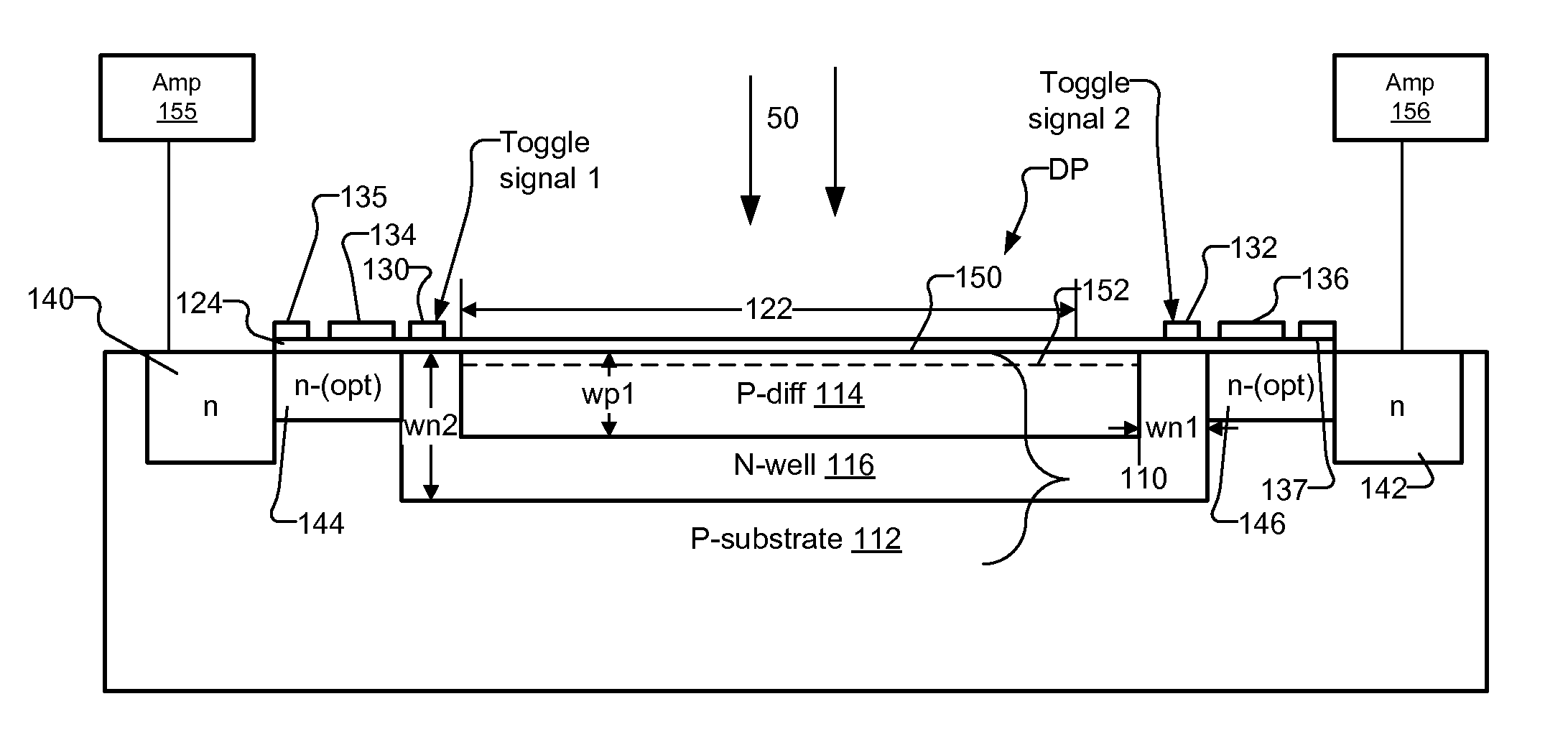
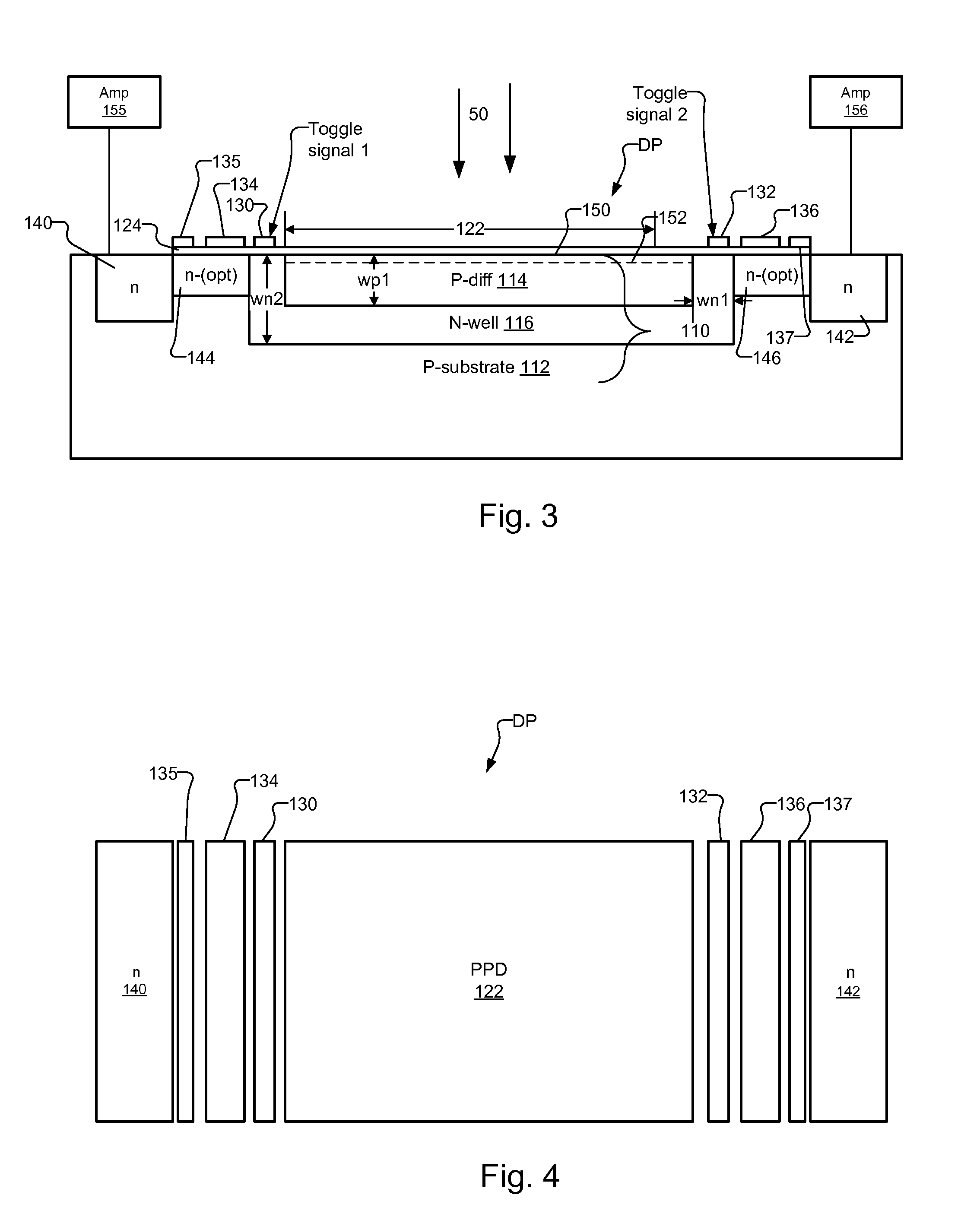
[0028]In the following descriptions, we use just p doped substrates in order to keep the descriptions clear and well-structured. However, the devices are not limited to p-doped substrates. In the case that n-doped material is used as substrate, all doping concentrations and considerations of the potential distributions are reversed, which, however, does not mean that any functioning of the device would be restricted.

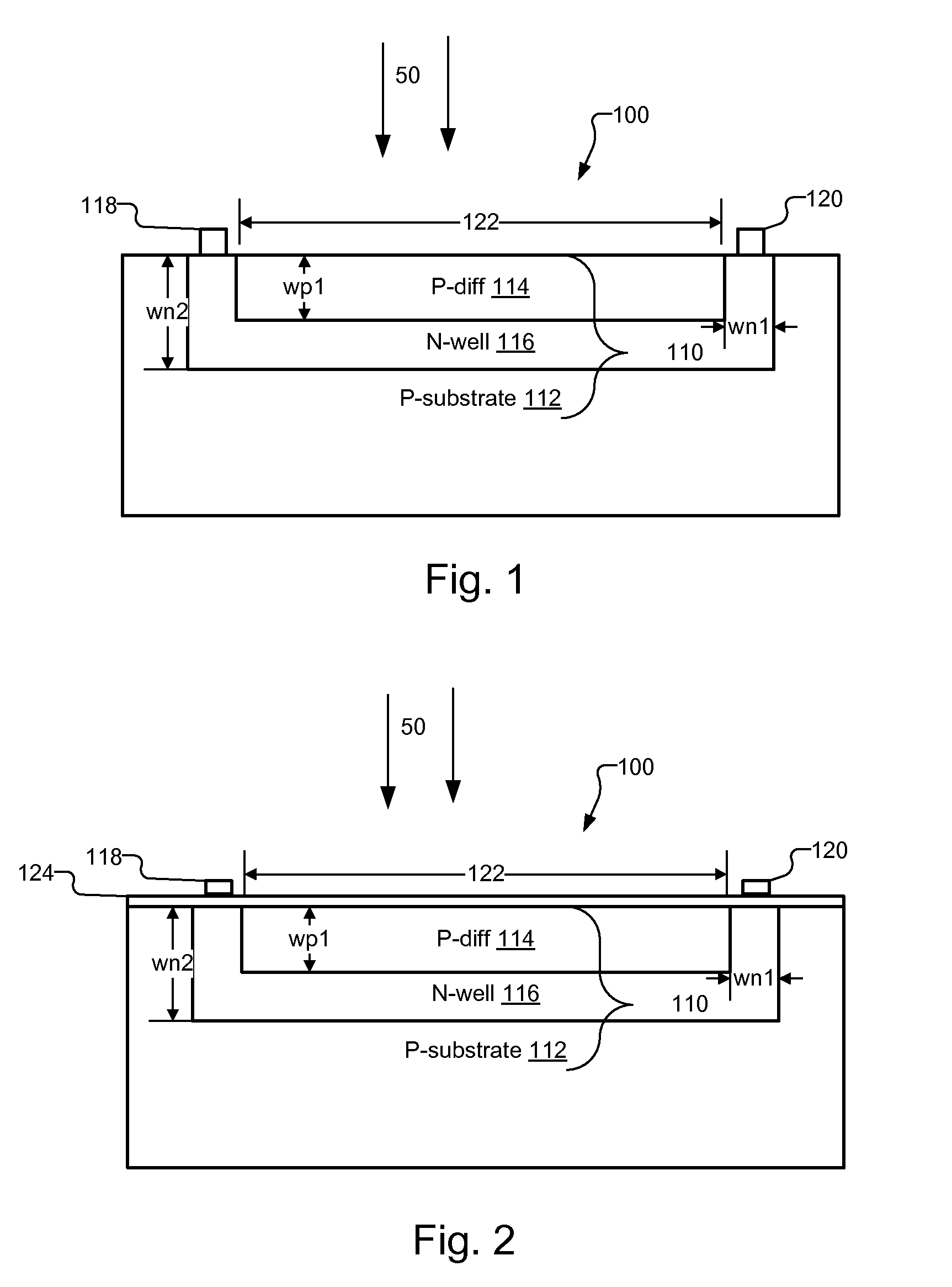
[0029]FIG. 1 shows the basic idea of a gate-less static drift field pixel 100 based on a pinned photodiode (PPD) structure. A pnp structure 110 is created, which is fully depleted when the two p-layers, p-doped substrate 112 and p-doped diffusion layer 114 are connected to the same potential and the sandwiched n-well layer 116 is set to a potential greater or equal the built-in voltage.

[0030]In the case that two different voltages are applied to the left (low potential) contact 118 and right (high potential) contact 120 to the n-well layer of the PPD structure 110, a con...


PUM


Abstract

A pixel based on a pinned-photodiode structure that creates a lateral electric drift field. The combination of the photodiode with adjacent CCD gates enables the utilization of the drift field device in applications such as 3-D imaging. Compared with recently used demodulation devices in CCD or CMOS technology, the new pinned-photodiode based drift field pixel has its advantages in its wide independence of the quantum efficiency on the optical wavelength, its high optical sensitivity, the opportunity of easily creating arbitrary potential distributions in the semiconductor, the straight-forward routing capabilities and the generation of perfectly linear potential distributions in the semiconductor.

Description

RELATED APPLICATIONS[0001]This application claims the benefit under 35 USC 119(e) of U.S. Provisional Application No. 61 / 033,501, filed on Mar. 4, 2008, which is incorporated herein by reference in its entirety.BACKGROUND OF THE INVENTION[0002]The demodulation of modulated light signals at the pixel level requires the switching of a photo-generated charge. While it is possible to use either photo-generated electrons or holes, typical solutions use photo-generated electrons because of their higher mobility in the semiconductor material. Some pixel architectures do the necessary signal processing based on the photo-current whereas other architectures work in the charge domain directly.[0003]Common to all pixels is the necessity to transfer charges through the photo-sensitive detection region to a subsequent storage area and / or to a subsequent processing unit. In the case of charge-domain based pixel architectures, the photo-charges are generally transferred to a storage or integration...

Claims


Application Information

Patent Timeline
Patent Type & Authority Applications(United States)
IPC IPC(8): H01L27/00H04N13/04G01S7/4914G01S17/894
CPCG01S17/89H01L27/14641G01S7/4914H01L27/14609G01S17/894
Inventor BUETTGEN, BERNHARDLEHMANN, MICHAELFELBER, JONAS
Owner HEPTAGON MICRO OPTICS
Why Eureka
Try Eureka