Substrate treatment apparatus, and substrate treatment method

a substrate treatment and substrate technology, applied in the field of substrate treatment apparatus and a, can solve the problems of uneven treatment of reduced etching power of the etching liquid, and difficulty in replacing the etching liquid present on the upper surface of the wafer with the newly supplied etching liquid, and achieve the effect of higher ra

Active Publication Date: 2009-08-06
DAINIPPON SCREEN MTG CO LTD
View PDF7 Cites 18 Cited by
  • Summary
  • Abstract
  • Description
  • Claims
  • Application Information

AI Technical Summary

Benefits of technology

[0011]It is an object of the present invention to provide a substrate treatment apparatus and a substrate treatment method which are capable of uniformly performing an etching treatment at a higher rate on the entire major surface of a substrate.

Problems solved by technology

Thus, the peripheral portion of the upper surface of the wafer is etched at a higher etching rate than the center portion, resulting in uneven treatment of the upper surface of the wafer.
Unless the deactivated etching liquid is properly replaced with newly supplied etching liquid on the upper surface of the wafer, the deactivated etching liquid and the newly supplied etching liquid are mixed with each other on the upper surface of the wafer, resulting in reduced etching power of the etching liquid.
This makes it difficult to replace the etching liquid present on the upper surface of the wafer with the newly supplied etching liquid.
This further reduces the etching rate.

Method used


Image

  • Substrate treatment apparatus, and substrate treatment method
  • Substrate treatment apparatus, and substrate treatment method
  • Substrate treatment apparatus, and substrate treatment method

Examples


first embodiment

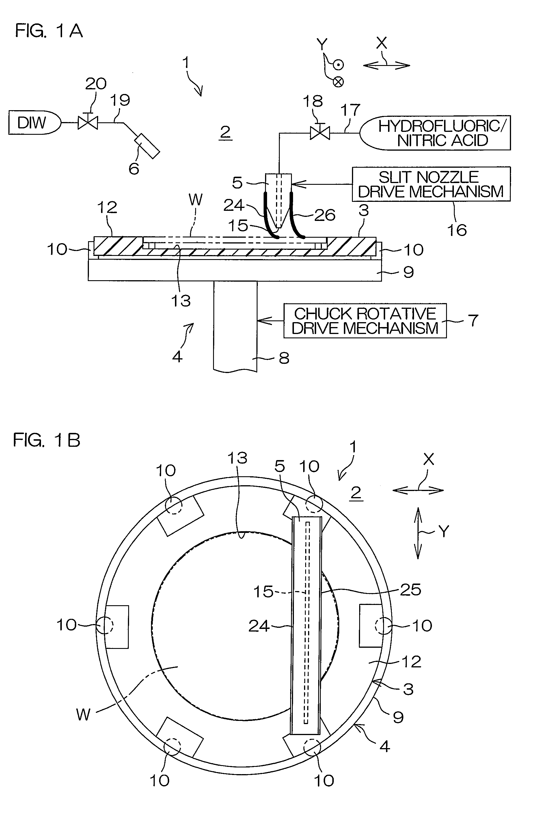
[0053]FIG. 1A is a sectional view schematically showing the construction of a substrate treatment apparatus 1 according to one embodiment (first embodiment) of the present invention. FIG. 1B is a plan view schematically showing the construction of the substrate treatment apparatus 1 shown in FIG. 1A.

[0054]The substrate treatment apparatus 1 is of a single substrate treatment type which performs an etching treatment on a back surface (upper surface) opposite from a front surface (device formation surface) of a round wafer W such as a silicon wafer for thinning the wafer W. In this embodiment, hydrofluoric / nitric acid (a mixture of hydrofluoric acid and nitric acid) is used as an etching liquid.

[0055]The substrate treatment apparatus 1 includes a substrate support (susceptor) 3 which generally horizontally holds the wafer W, a spin chuck 4 which holds the substrate support 3 and rotates the wafer W and the substrate support 3 about a vertical axis extending through the center of the w...

second embodiment

[0105]In the second embodiment, the slit nozzle 5 is attached to an arm 61 generally horizontally extending above the spin chuck 4. The arm 61 is supported by an arm support shaft 62 generally vertically extending on a lateral side of the spin chuck 4. An arm pivot drive mechanism 63 is connected to the arm support shaft 62. The arm support shaft 62 is pivoted by a driving force of the arm pivot drive mechanism 63, whereby the arm 61 is pivoted.

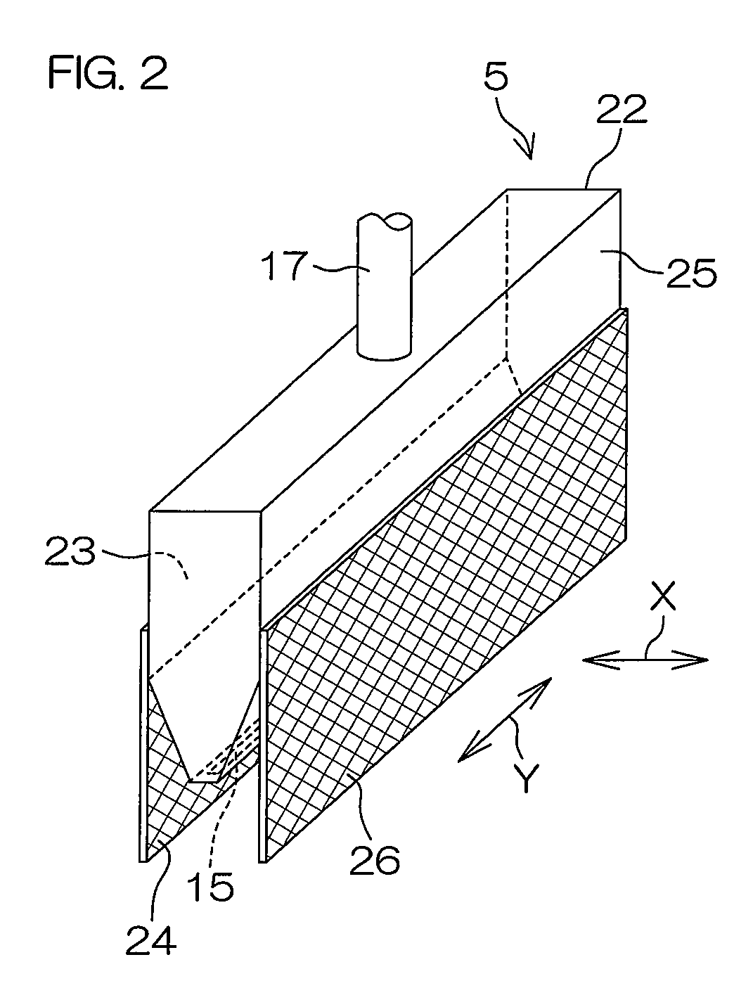
[0106]When the arm 61 is pivoted by driving the arm pivot drive mechanism 63, the slit nozzle 5 is reciprocally moved horizontally between a scan start position P3 located outside the upper region of the substrate support 3 (as indicated by a solid line in FIG. 7) and a return position P4 angularly spaced 90 degrees from the scan start position P3 about the rotation center of the wafer W outside the upper region of the substrate support 3. Since the first sheet 24 and the second sheet 26 each have a sheet length that is greater than the diame...

third embodiment

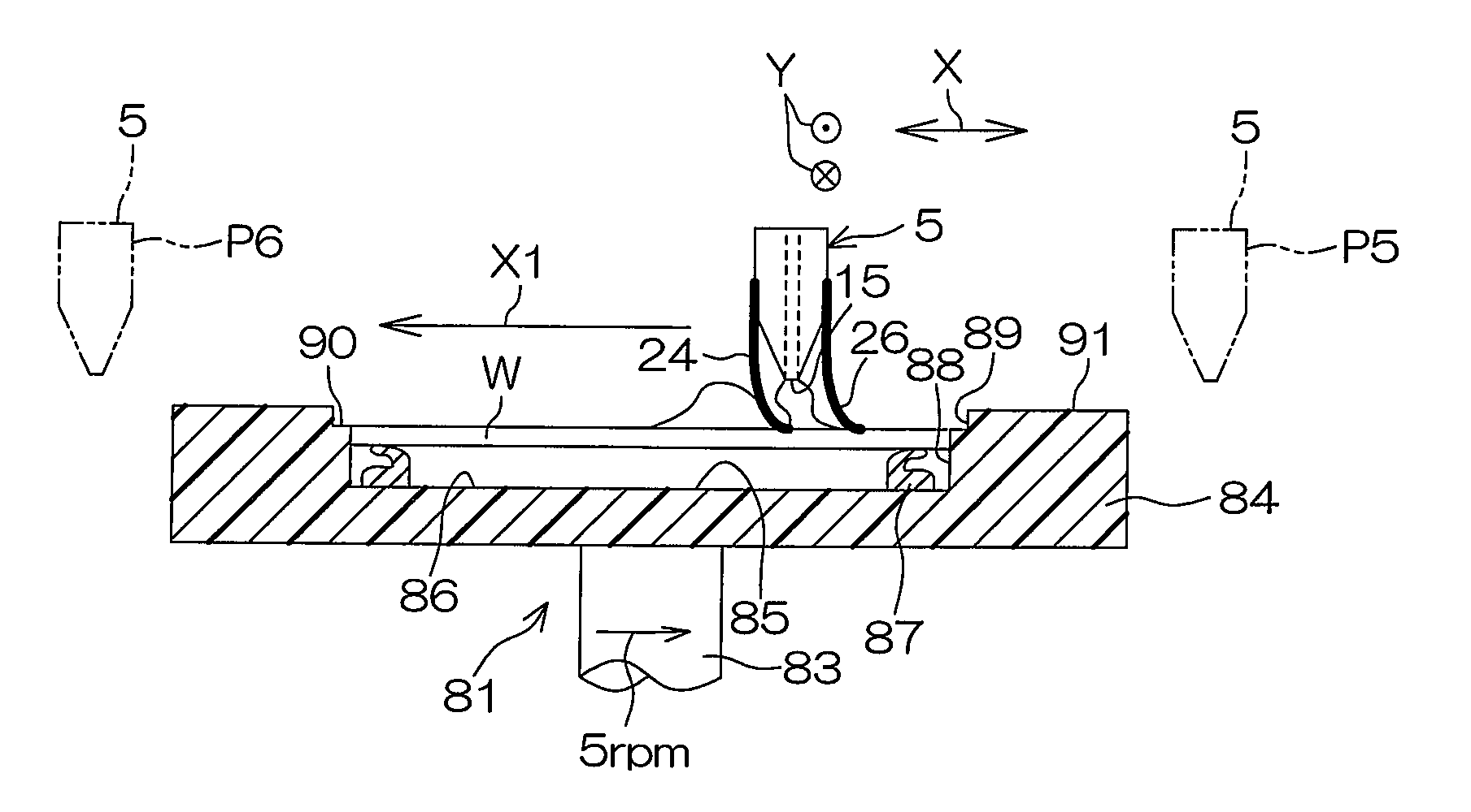
[0110]In the third embodiment, a substrate holding mechanism 81 is employed as substrate holding mechanism instead of the substrate support 3 and the spin chuck 4. The substrate holding mechanism 81 holds and rotates the wafer W.

[0111]The substrate holding mechanism 81 includes a disk-shaped spin base 84 (base member) fixed to an upper end of a rotation shaft 83 which is rotated about a vertical axis by a rotative drive force of a rotative drive mechanism (substrate rotating mechanism) 82. The spin base 84 is formed of polyvinyl chloride, and has a flat upper surface 91.

[0112]The spin base 84 has a hollow cylindrical accommodation recess 85 provided in a center portion of an upper surface thereof for accommodating the wafer W. An annular seal member 87 serving as a support member for supporting the wafer W is provided along a peripheral edge of a bottom 86 of the accommodation recess 85 on an upper surface of the bottom 86. The lower surface of the wafer W is supported by the seal m...


PUM

PropertyMeasurementUnit
diameteraaaaaaaaaa
widthaaaaaaaaaa
flow rateaaaaaaaaaa

Abstract

The substrate treatment apparatus according to the present invention includes a substrate holding mechanism which holds a substrate, a nozzle body having a spout which spouts an etching liquid toward a major surface of the substrate held by the substrate holding mechanism, a nozzle body movement mechanism which moves the nozzle body in a predetermined movement direction so as to move an etching liquid application position at which the etching liquid is applied on the major surface, a first flexible sheet attached to the nozzle body to be brought into contact with a portion of the major surface located on one of opposite sides of the etching liquid application position with respect to the movement direction, and a second flexible sheet attached to the nozzle body to be brought into contact with a portion of the major surface located on the other side of the etching liquid application position with respect to the movement direction.

Description

BACKGROUND OF THE INVENTION[0001]1. Field of the Invention[0002]The present invention relates to a substrate treatment apparatus and a substrate treatment method for performing an etching treatment to etch a major surface of a substrate with an etching liquid. Examples of the substrate to be subjected to the etching treatment include semiconductor wafers, glass substrates for liquid crystal display devices, glass substrates for plasma display devices, substrates for FED (Field Emission Display) devices, substrates for optical disks, substrates for magnetic disks, substrates for magneto-optical disks, and substrates for photo masks.[0003]2. Description of Related Art[0004]In semiconductor device production processes, a liquid treatment is often performed to treat a semiconductor wafer (hereinafter referred to simply as “wafer”) with a treatment liquid. An exemplary liquid treatment is an etching treatment which is performed by supplying an etching liquid to a major surface of the waf...

Claims


Application Information

Patent Timeline
Patent Type & Authority Applications(United States)
IPC IPC(8): C23F1/00C23F1/08
CPCB05C5/0254H01L21/6708B05C11/08B05C11/04G03F1/80A63B67/045A63B71/04A63B61/04
Inventor NADA, KAZUNARIARAI, KENICHIRO
Owner DAINIPPON SCREEN MTG CO LTD
Why Eureka
Try Eureka